This paper introduces how system-in-package SiP integrates multiple integrated circuit chips and other discrete components into the same package, which effectively solves the problems of bandwidth, interconnection delay, power consumption and integration faced by traditional packaging. At the same time, compare SiP with system on a chip SoC, and point out their respective characteristics and development trends.
Liu ling, Zheng Xueren, Li Bin
(Special Integrated Circuit Research and Design Center, Department of Applied Physics, South China University of Technology)
Abstract:This paper introduces how system-in-package SiP integrates multiple integrated circuit chips and other discrete components into the same package, which effectively solves the problems of bandwidth, interconnection delay, power consumption and integration faced by traditional packaging. At the same time, compare SiP with system on a chip SoC, and point out their respective characteristics and development trends.
1 IntroductionThe traditional electronic system is divided into three levels: I C integration, package integration and board-level structure. Integrated circuit has entered the era of system integration, and SoC will be the mainstream technology in the future. Large-scale integrated circuits not only improve the integration level, but also reduce the interconnection delay, which makes the bottleneck limiting the system performance shift from chip level to package level. The effective way to solve the packaging bottleneck problem is to optimize the whole electronic system from the system point of view, and take the packaging factors into account in the design stage of the chip. Therefore, it is very important to study the system-level packaging problem with a brand-new concept. The system in package (SIP) discussed in this paper is a packaging technology with high integration, low cost and high performance.
2 SiP and its performance descriptionThe packaging technology is more and more new every ten years. From the first generation of socket components, the second representative surface mounting, the third generation of area array to the fourth generation of chip packaging, packaging contractors and chip manufacturers have worked closely together to research and develop several advanced packaging and testing technologies to meet the needs of different fields. These emerging new packaging technologies have laid a solid foundation for the realization of SiP [1]. SiP refers to manufacturing a number of bare chips and micro passive components by different technologies on the same small substrate, forming high-performance micro components with system functions. It has a series of performance characteristics:
(1) Individual chips or devices can be upgraded flexibly and timely, thus shortening the design cycle of IC, reducing the design cost and chip testing time.
(2) With the advanced substrate preparation technology, a new bus standard similar to on-chip bus can be quickly adopted, and the high-speed and low-noise interconnection technology provided by SiP can be fully utilized.
(3) The bandwidth of data transmission on the system bus is directly proportional to the clock frequency f and the data width w.. Compared with board-level wiring, the length of interconnection leads between dies in SiP package is shorter, which effectively reduces the interconnection delay and crosstalk of the system, reduces the capacitive reactance, and enables the device to work at a higher working frequency, thus effectively improving the bandwidth. Shorter interconnection between dies will also bring some potential benefits: the IO output of dies does not need to adopt strong driving design, and the integrity of signals transmitted between dies can be ensured by using low-power IO buffer, so lower working voltage can be adopted, thus further reducing the power consumption of devices. In addition, it can also reduce the power supply and grounding pins introduced to shield parasitic capacitance and inductance caused by high-speed signal pins, and reduce the number of I/O pins between P C B and PCB.
(4) SiP can be used as a standard unit for PCB assembly, and it can also be the final electronic product, such as removable flash memory card. Different from traditional chip packaging, SiP can not only deal with digital systems, but also be used in optical communication, sensors and MEMS. In the next decade, electronic components, subsystems or systems encapsulated by SiP will be widely used in computer, automation, communication and other fields.
2.1 System Integration Scheme: Comparison between SiP and SoC
With the continuous expansion of chip scale, a complete electronic system can be integrated into one chip, namely system on a chip SoC. SoC has many advantages, such as high performance, low power consumption and small size, and it is the main direction of the development of the next generation integrated circuits. However, SoC still faces many limiting factors in practical application, including insufficient IP resources, high R&D cost, long design cycle, complex production process and low yield. In addition, there are problems in using hybrid semiconductor technologies (such as GaAs and SiGe) in SoC.
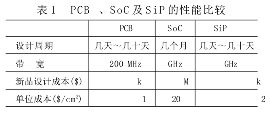
SiP packages multiple ics and passive components on a high-performance substrate to form a system, which can be easily compatible with chips with different manufacturing technologies. For example, traditional C M O S silicon chips can be used for computing logic, and SiC, SiGe and GeAs chips can be used for R&F and high-power circuits, so that the packaging can enter the system integration level from the single chip level. The area occupied by SiP is much smaller than that occupied by discrete package, and the cost is similar to that of a single discrete package. In terms of test cost, DFT design is needed in the design of SoC devices, which increases the test cost and design time. SiP adopts the traditional IC test flow, and only needs to add JTAG test to the bus in the package, which is the common requirement of PCB board. Table 1 compares the performance and factors of SoC, SiP and PCB.
In fact, SiP and SoC are not mutually opposite technologies. They provide solutions for different levels of electronic systems and adapt to the choice of target markets. SoC is applied to the relatively high-end market, and SiP is applied to the mid-end market with its high cost performance. In the foreseeable future, SoC and SiP can complement each other and will coexist for a long time.
2.2 SiP or MCM, who will be the next generation packaging scheme [2]
MCM fixes multiple dies on a substrate and connects them together. A typical MCM package may contain more than a dozen dies. The main disadvantage of MMC is the cost, which leads to its main application in military, aerospace or high-performance electronic products that don't care much about price factors. Compared with MCM, SiP technology is more mature. It does not simply assemble bare chips into a multi-chip module, but carefully divides the functions in the early stage of functional design to determine which chips can realize these functions respectively. The chip in SiP is ASIC or chip-based IP, which is an integrated system of multiple components optimized for a system-level package. At the same time, SiP adopts mature high-density interconnection technology such as BGA or FC, and realizes the functions of passive devices such as high Q inductor and bypass capacitor efficiently in the package. SiP improves performance and reduces cost, which builds a bridge to applications. All these indicate that SiP represents the future development trend of packaging technology, not M C M
2.3 SiP package inter-chip bus performance [3]
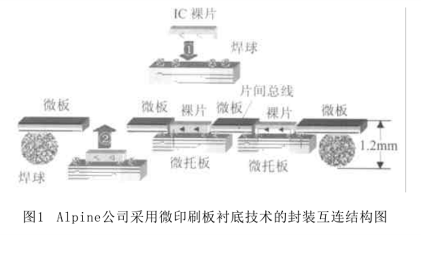
SiP can provide system-level connection with low power consumption and low noise, and work at higher frequencies to obtain wider bandwidth. For example, Al-pine's microplate substrate technology (as shown in Figure 1), using the existing semiconductor technology to prepare the substrate, very fine line width and accurate perforation position can be obtained. Using copper interconnects on low K dielectric can provide very rich connecting wire resources, and the chips in close proximity can reduce the bus length and capacitance between chips, and the parasitic inductance of the power line distribution network connected to the device is also small, which provides the basis for adopting the new bus standard in the package.
The system bus on PCB board mostly adopts multiplexing technology to reduce the number of IO. However, multiplexing will increase the signal transmission delay, and the frequent signal conversion of the bus also increases the power consumption of the system. Non-multiplexing bus is used between chips in SiP, which separates the input and output paths and effectively avoids competition and adventure. This bus standard has long been adopted in the chip, but it is rarely used outside the chip. SiP's new micro-substrate technology can use abundant connecting wire resources, and the IO driving unit between chips is also different from the inside of chips and PCB boards, as shown in Figure 2. In single-chip mode, the signal is output to the PCB through the driving unit, and in multi-chip mode, the signal is directly output to the internal bus of SiP. It can be seen that the voltage and current of this programmable IO driver module can be adjusted, which is beneficial to reduce power consumption. Furthermore, if the routing of SiP can be synchronized with the chip, the optimization effect is the greatest, and even the voltage of the inter-chip bus is close to the voltage in the chip, the clock line delay can be reduced. The high-performance interconnection of SiP substrate ensures the integrity of low-drive transmission signals, and is also conducive to the formulation of new high-speed bus standards.
The performance of SiP inter-chip bus has become the key to improve the internal bus bandwidth of the system. By expanding the number of signal bits of the inter-chip connection and improving the working frequency, SiP can obtain a bus bandwidth similar to that of SoC. At the same time, the existing mature system bus standard can also be used as a compromise between chips, so that IC chips can be applied without major changes. Therefore, appropriate on-chip bus and inter-chip bus should be designed at the same time of adopting SiP technology to obtain the highest efficiency.
SiP of Alpine Company can reduce the inter-chip delay to 50ps/mm, which is similar to the RC delay of on-chip connection. Therefore, some new technologies, such as borrowing clock delay time, global asynchronous/local synchronization and self-timed, which used to be used only in the chip, can now be successfully adopted in SiP.
3 SiP encapsulation implementation technology [4]After analyzing and dividing the functions of the system, SiP chooses the appropriate technology to achieve the design performance of the system in the best way and at the lowest cost. It is worth noting that for SiP, the internal interconnection and pin location flexibility provided by advanced packaging technologies such as BGA and FC are also convenient for IC designers. Packaging design has become an integral part of IC process, and the method of chip/package joint design has replaced the traditional production process of chip+package+assembly.
Fig. 2 is a schematic diagram of Amkor's SuperFCTMSiP package, which packages a flip-chip high-speed ASIC processing chip, some memory chips and other passive components on the same high-density substrate for network routers and other devices. The signal is concentrated in the first and second layers of the high-density multilayer substrate, and the signal integrity can be guaranteed. At the same time, the package also saves space on P C B, which is beneficial to adding more functional units to PCB.
As a brand-new packaging form, there are three main ways to realize SiP: the first is the integration of passive components and active IC, that is, micro-component technology; The second is 3D packaging technology; The third type is wafer level package (W L P )[ 5].
3.1 Micro-component technology [6]
At a certain technical level, when the number of pins of the chip reaches saturation, it is necessary to increase the package size of the chip to meet the requirements of more leads, which contradicts the requirements of chip miniaturization. One of the solutions is to divide the system into several modules according to certain priorities, such as interconnection density, heat dissipation and signal integrity. Each module can make full use of its peripheral area as input and output, and the modules are interconnected by metal leads, that is, micro-component technology. Typical applications of micro-component technology include microcontrollers, D S P and SDRAM, F L A S H, R F fields and network routers. After division, the number of leads in the remaining part will be greatly reduced, and the whole electronic system can be realized by using relatively cheap substrates. Considering the cost, this method can't assemble too many devices, and the typical size should be less than 1 inch, with at most five active components. Micro-components should be transparent to users, no matter how many components are integrated inside them, users can use it like discrete devices. The characteristics of micro-component SiP are suitable for embedding passive components, including standard inductors. When the frequency exceeds 2 G H z, the geometric tolerance, consistency and repeatability of the component determine the quality factors of the device. Designers can use four parameters: diameter d, wire width w, wire spacing s and number of turns n to control the geometric dimensions and characteristics of embedded spiral inductors well, and ensure the consistency between performance and geometric parameters, thus obtaining high Q-value components.
3.2 3D package [7]
3 D packaging is a kind of advanced SiP packaging technology, which stacks and interconnects more than two bare dies in the direction perpendicular to the chip surface. it takes up less space and has stable electrical performance. Hybrid interconnection technology can be used in 3D package to adapt to the interconnection between different devices. For example, die to die, die to micro-substrate, die to passive components can be interconnected by flip chip and wire bonding as needed.
In traditional chip packaging, each die needs a corresponding high-density interconnection substrate, and the proportion of substrate cost to the manufacturing cost of the whole packaged device product is very high. Take BGA as an example, accounting for 40% ~ 50%. The substrate for Flip Chip is higher, reaching 70% ~ 80% [8]. Only one substrate is needed for multiple dies in 3D package. At the same time, because a large number of interconnections between dies are carried out in the package, the length of interconnection lines is greatly reduced, which improves the electrical performance of the device. 3D packaging can also reduce the number of pins by sharing IO ports. For example, 3D packaging devices with FLASH and SRAM stacked are widely used in portable telecommunication products, and more than 50% of IO can be shared. Amkor company saves 30% cost by stacking 3 bare dies in 3D packaging compared with single chip packaging.
3.3 wafer level package (W L P)
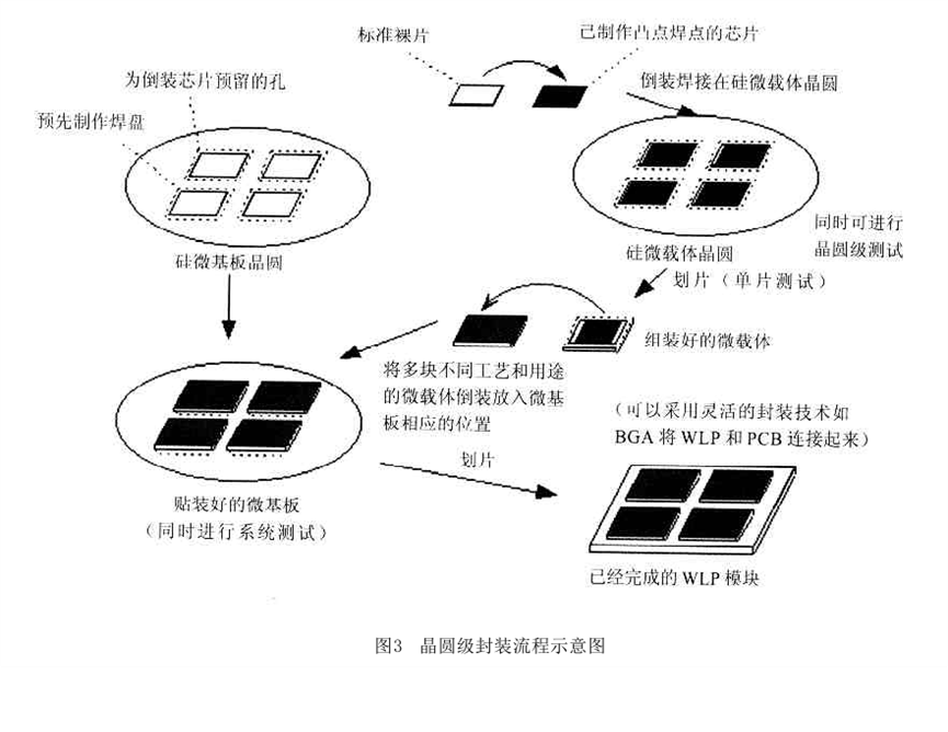
WLP can effectively improve the package integration, and usually adopts the flip-chip (FC) interconnection technology, which is the one with the smallest space occupation in CSP in chip scale package. The traditional packaging takes the diced single chip as the processing target, while WLP takes the wafer as the processing object, which is packaged and tested directly on the wafer, then cut into packaged IC, then grow metal bumps on the IC, stick them on the substrate or glass substrate with FC technology, and finally assemble them on the PCB. Fig. 3 is a schematic diagram of the WLP process of microcarriers and microplates using 3m copper wiring and low-k dielectric (ε r =2.65) technology of Alpine Microsystem, which effectively reduces the unit resistance and capacitance of interconnection lines (even lower than the interconnection in a 0.5µm VLSI chip), so it can achieve higher performance.
The whole manufacturing process of WLP packaging is completed in the wafer factory, so that the packaging and testing of chips are integrated into the wafer production process. From here, we can see an interesting phenomenon: driven by cost minimization, the vertical division system of IC industry may tend to merge, and the same manufacturer will produce, package and test chips (such as W L P), thus optimizing production costs, sharing marketing networks and other resources, and reducing technological processes (especially similar technological processes). The two opposite trends, integration and continuous subdivision of IC production process, exist at the same time, which will ultimately depend on the cost factor of the whole production system.
4 ConclusionSiP package provides a widely used and economical package scheme for designers, which can embed IC made by different processes, embed and integrate passive devices, even optical devices and micromechanical MEMS, and provide users with compact and excellent functional modules. SiP based on systematic design idea conforms to the future development direction and has a broad application market.
Because SiP is a new technology, the corresponding design software does not support it enough. However, with the solution of key technologies and the wide application in portable devices such as mobile phones and PDA, SiP packaging is expected to grow rapidly in the next decade.
About Maxipcb
Maxipcb empowers innovators to turn cutting-edge technologies into reality.
We offer one-stop solutions for design, simulation, testing, PCB manufacturing, component procurement and SMT assembly, enabling efficient development, rapid deployment and risk control across the full product lifecycle.Serving the world in communications, industrial automation, aerospace, automotive, semiconductor and beyond, we build a safer, more connected future together. 


