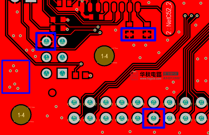
After all the design contents of PCB are designed, the last key step-copper laying is usually carried out. Copper laying is to cover the idle space on PCB with copper surface. All kinds of PCB design software provide intelligent copper laying function. Usually, the area after copper laying will turn red, which means that this part of the area is covered with copper.
After all the design contents of PCB are designed, the last key step-copper laying is usually carried out. Copper laying is to cover the idle space on PCB with copper surface. All kinds of PCB design software provide intelligent copper laying function. Usually, the area after copper laying will turn red, which means that this part of the area is covered with copper.
So, why did you finally lay copper? Can't it be paved? For PCB, copper coating has many functions, such as reducing ground impedance and improving anti-interference ability; Connect with the ground wire to reduce the loop area; And help heat dissipation, and so on.
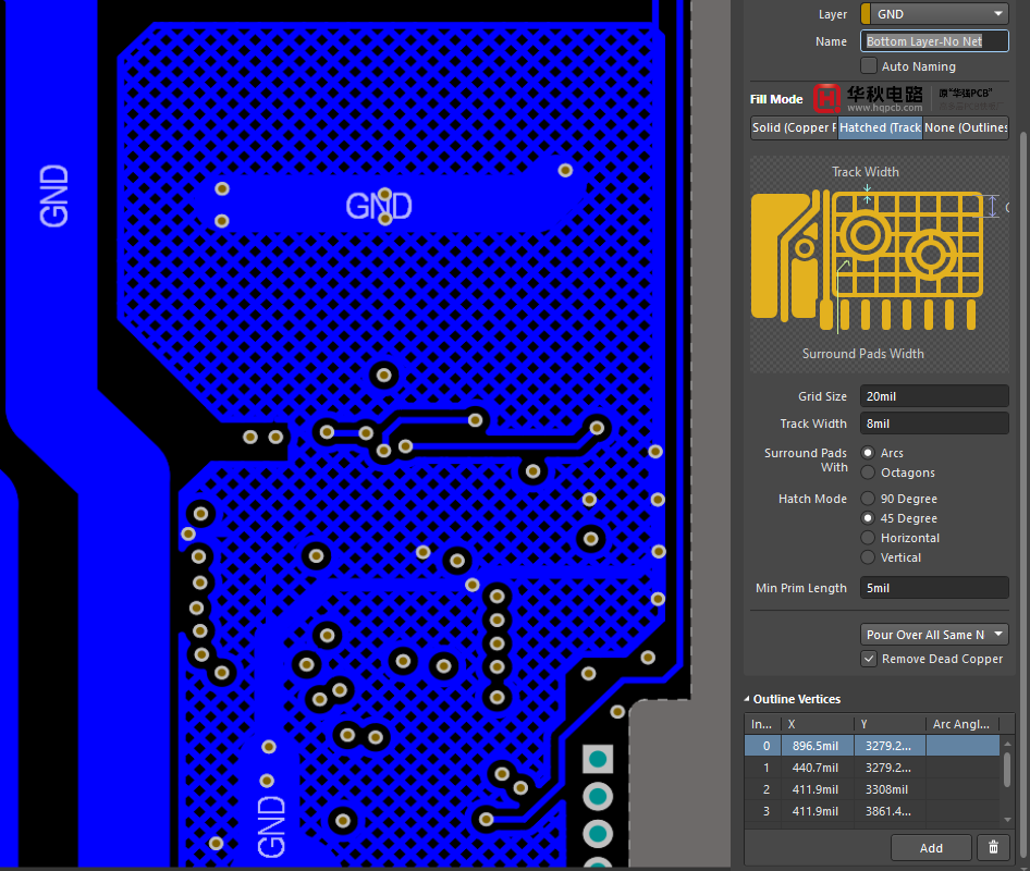
1. Laying copper can reduce the impedance of ground wire, and provide shielding protection and noise suppression. There are a lot of spike pulse currents in digital circuits, so it is more necessary to reduce the ground impedance. Copper plating is a common method to reduce the ground impedance. Copper laying can reduce the resistance of ground wire by increasing the conductive cross-sectional area of ground wire; Or shorten the length of the ground wire and reduce the inductance of the ground wire, thus reducing the impedance of the ground wire; It is also possible to control the capacitance of the ground wire, so that the capacitance value of the ground wire can be appropriately increased, thereby improving the conductivity of the ground wire and reducing the impedance of the ground wire. A large area of ground or power supply copper can also play a shielding role, which is helpful to reduce electromagnetic interference, improve the anti-interference ability of the circuit and meet the requirements of EMC. In addition, for high-frequency circuits, copper plating provides a complete return path for high-frequency digital signals, reducing the wiring of DC network, thus improving the stability and reliability of signal transmission.
2. Laying copper can improve the heat dissipation capacity of PCB.
In PCB design, laying copper can be used not only to reduce the ground impedance, but also to dissipate heat. As we all know, metal is easy to conduct electricity and heat, so if the PCB is covered with copper, there will be more metal components in other blank areas such as gaps in the board, and the heat dissipation surface area will increase, so it is easy to dissipate heat of the PCB as a whole. Spreading copper can also help to distribute heat evenly and prevent the occurrence of local high temperature areas. By evenly distributing heat to the whole PCB board, local heat concentration can be reduced, the temperature gradient of heat source can be reduced, and the heat dissipation efficiency can be improved. Therefore, in the PCB design, you can use copper to dissipate heat in the following ways:
- Design heat dissipation area: according to the distribution of heat sources on PCB, design heat dissipation areas reasonably, and lay enough copper foil in these areas to increase heat dissipation surface area and heat conduction path.
- Increasing the thickness of copper foil: increasing the thickness of copper foil in the heat dissipation area can increase the heat conduction path and improve the heat dissipation efficiency.
- Design heat dissipation through hole: design heat dissipation through hole in heat dissipation area, and conduct heat to the other side of PCB through the through hole, so as to increase heat dissipation path and improve heat dissipation efficiency.
- Adding heat sinks: add heat sinks in the heat dissipation area to conduct heat to the heat sinks, and then dissipate heat through natural convection or fan radiator to improve heat dissipation efficiency.
3. Laying copper can reduce the deformation and improve the manufacturing quality of PCB. Laying copper can help to ensure the uniformity of electroplating and reduce the deformation of plates in the lamination process, especially for double-sided or multi-layer PCB, and improve the manufacturing quality of PCB.
If there are too many copper foils in some areas and too few in some areas, it will lead to uneven distribution of the whole board, and laying copper can effectively reduce this gap.
 4. Meet the installation requirements of special devices.
 For some special devices, such as devices that need grounding or special installation requirements, copper laying can provide additional connection points and fixed support, and enhance the stability and reliability of devices. Therefore, based on the above advantages, in most cases, electronic designers will lay copper on PCB boards. However, laying copper is not a necessary part in PCB design. In some cases, copper laying may not be suitable or feasible. The following are some cases where it is not suitable to lay copper:
① High-frequency signal lines: For high-frequency signal lines, laying copper may introduce additional capacitance and inductance, which will affect the signal transmission performance. In high frequency circuits, it is usually necessary to control the routing mode of the ground wire and reduce the return path of the ground wire, rather than over-laying copper. For example, laying copper will affect some signals of the antenna. Placing copper in the area around the antenna is easy to cause the signal collected by weak signals to receive relatively large interference. The antenna signal is very strict in setting the parameters of the amplifier circuit, and the impedance of copper laying will affect the performance of the amplifier circuit. Therefore, the surrounding area of the antenna part is generally not covered with copper.
② High-density circuit board: For high-density circuit boards, excessive copper laying may lead to short circuit or grounding problems between lines, which will affect the normal operation of the circuit. When designing high-density circuit boards, it is necessary to carefully design the copper-paved structure to ensure sufficient spacing and insulation between lines to avoid problems.
③ Too fast heat dissipation and difficult welding: If the pins of components are covered with copper, it may lead to too fast heat dissipation, which makes it difficult to disassemble and repair. We know that the thermal conductivity of copper is very high, so whether it is manual welding or reflow welding, the copper surface will conduct heat quickly during welding, resulting in the loss of temperature such as soldering iron, which has an impact on welding. Therefore, the "cross-shaped pad" is used as far as possible in design to reduce heat dissipation and facilitate welding.
④ Special environmental requirements: In some special environments, such as high temperature, high humidity and corrosive environment, copper foil may be damaged or corroded, thus affecting the performance and reliability of PCB. In this case, it is necessary to choose suitable materials and treatment methods according to specific environmental requirements, rather than over-laying copper.
⑤ Special-level boards: For boards with special levels, such as flexible printed circuit board and rigid-flexible composite boards, it is necessary to carry out copper laying design according to specific requirements and design specifications to avoid the problem of flexible layer or rigid-flexible composite layer caused by excessive copper laying.
To sum up, in PCB design, it is necessary to make appropriate choices between laying copper and not laying copper according to specific circuit requirements, environmental requirements and special application scenarios.About Maxipcb
Maxipcb empowers innovators to turn cutting-edge technologies into reality.
We offer one-stop solutions for design, simulation, testing, PCB manufacturing, component procurement and SMT assembly, enabling efficient development, rapid deployment and risk control across the full product lifecycle.Serving the world in communications, industrial automation, aerospace, automotive, semiconductor and beyond, we build a safer, more connected future together. 

