Switching power supply is a power converter with power MOS as the core. Besides the parameters of the chip itself will have a great impact on the power quality, the design of PCB is also very important.
Switching power supply is a power converter with power MOS as the core. Besides the parameters of the chip itself will have a great impact on the power quality, the design of PCB is also very important.
Today, taking a simple Buck circuit as an example, we will share with you some design experiences about copper laying on the PCB at the switch side from different angles.
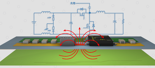
First of all, the switch side, which we often say is SW, is a very key position in Buck circuit, which is the intersection of input loop and output loop, and also the place where the bridge power MOS is directly connected.
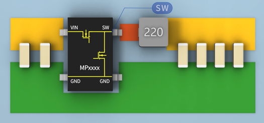
Generally speaking, the copper area of PCB for signals connected with power MOS should be designed as large as possible, mainly considering two aspects:
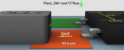
On the one hand, the power loop needs to run a large current. At the same distance, increasing the width of copper paving can increase the current capacity of the wiring and reduce the path loss.
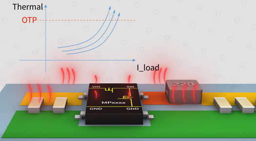
On the other hand, the copper pad directly connected with the power MOS also plays the role of device heat dissipation. As we know, the heat dissipation capacity will often become the bottleneck of the output capacity of power chips. Because of the good thermal conductivity of the pin pin of the chip, the thermal resistance from the chip core to the PCB is often smaller than that to the packaging surface, which means that most of the heat of the chip is dissipated after being introduced into the PCB through the pin pin pin of the chip, so increasing the copper laying area of SW will also improve the heat dissipation capacity of Buck chip to a certain extent.
However, does this mean that the bigger the copper spread of SW, the better?
The answer is no.
If viewed from the noise dimension, SW takes over the input loop and output loop of Buck topology. With the switching of MOS, the voltage at SW will also change periodically. At the same time, the current of SW fluctuates regularly with the high frequency switching of MOS.
When the copper area of SW becomes larger, the parasitic capacitance to the reference ground will also increase, and the noise caused by high-frequency voltage fluctuation will be more easily coupled to the reference ground through the parasitic capacitance, thus affecting the identification of other sampling signals.
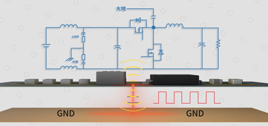
At the same time, the changing current will produce a changing magnetic field in space. When the magnetic wire passes through the closed coil, it will induce voltage noise, which will have a certain impact on the nearby signals. With the increase of copper area, the radiation range of interference will be wider.
Therefore, in order to minimize the impact on peripheral signals, we hope that the smaller the copper laying area of SW, the better.
In addition, we don't recommend drilling holes in SW.
In practical application, in order to reduce the influence of power supply noise on the signal chain, we will add a complete GND layer under the power supply layer as a noise shielding layer. Once the via hole is added at SW, the integrity of the shielding layer will be broken, and the noise will interfere with the signal transmission of other layers along the via hole.
So, how to solve the above contradiction?
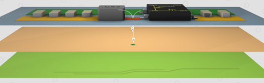
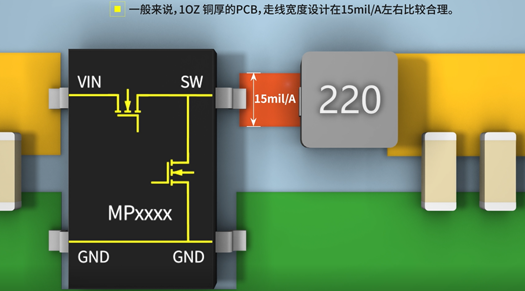
The width of 1SW copper laying needs to ensure that the cross section has enough current capacity, which is the first condition. Generally speaking, it is reasonable to design the trace width of a 1OZ copper-thick PCB at about 15 mil/a. On this basis, the distance between SW and inductor is shortened as much as possible to reduce the interference to peripheral signals.
2 We can improve the heat dissipation capacity of MOS by increasing the copper-laying area of power supply chip GND and input copper-laying area. In this way, this design contradiction can be skillfully resolved.
About Maxipcb
Maxipcb empowers innovators to turn cutting-edge technologies into reality.
We offer one-stop solutions for design, simulation, testing, PCB manufacturing, component procurement and SMT assembly, enabling efficient development, rapid deployment and risk control across the full product lifecycle.
Serving the world in communications, industrial automation, aerospace, automotive, semiconductor and beyond, we build a safer, more connected future together.


