For PCB engineers, have you ever wondered why the PCB ground (GND) is connected to a metal enclosure through a resistor and a capacitor?
For PCB engineers, have you ever wondered why the PCB ground (GND) is connected to a metal enclosure through a resistor and a capacitor?
Abstract
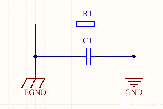
Grounding is a perennial topic in electronic product design. This article focuses on a specific aspect: the grounding between metal enclosures and PCBs. In many system designs, we often see the PCB ground (GND) connected to the metal enclosure ground (EGND) via a high-voltage capacitor C1 (1~100nF/2KV) in parallel with a high-value resistor R1 (1MΩ). This article explains the design rationale behind this configuration.
1 Function of the Capacitor
From the perspective of EMS (Electromagnetic Susceptibility), on the premise that the protective earth (PE) is reliably connected to the earth, this capacitor is designed to reduce the impact of high-frequency interference signals (referenced to earth potential) on the circuit, thereby suppressing the instantaneous common-mode voltage difference between the circuit and the interference source.
Ideally, directly connecting GND to PE would be the best solution, but direct connection may cause operational difficulties or potential safety hazards (e.g., the GND generated after a rectifier bridge cannot be directly connected to PE). Thus, a path is designed that blocks low-frequency signals but allows high-frequency signals to pass through.
From the perspective of EMI (Electromagnetic Interference), if the metal enclosure is connected to PE, this high-frequency path also helps prevent high-frequency signals from radiating into the external environment.
Capacitors conduct alternating current (AC) and block direct current (DC), and their specific roles in this configuration are as follows:
- When the enclosure is well earthed: It suppresses the dynamic common-mode voltage between high-frequency interference sources and the circuit (EMS); meanwhile, it forms a high-frequency discharge path, allowing high-frequency noise generated inside the PCB to flow through the capacitor to the enclosure and then to the earth, avoiding antenna radiation of high-frequency interference (EMI).
- When the enclosure is not reliably earthed (e.g., no earth wire, dry soil around the grounding rod): The enclosure potential may be unstable or carry static electricity. Direct connection between the PCB and the enclosure could damage PCB chips. The capacitor isolates low-frequency high voltage and static electricity, protecting the PCB from damage.
Component selection for the capacitor: Y-capacitors or high-voltage film capacitors are recommended, with a capacitance value ranging from 1nF to 100nF.
2 Function of the Resistor
This resistor effectively protects the PCB from damage caused by ESD (Electrostatic Discharge).
If the PCB ground is connected to the enclosure ground only via a capacitor, the PCB forms a floating ground system. During ESD testing or operation in a complex electromagnetic field, injected charges cannot be effectively released and will accumulate on the PCB. When the accumulated charge exceeds the breakdown voltage of the weakest insulation point between the PCB and the enclosure, a discharge occurs—this can generate tens to hundreds of amperes of current in an extremely short time, causing the circuit to malfunction due to electromagnetic pulses or damaging components near the discharge point.
Adding this resistive component enables gradual charge release and high-voltage elimination. According to the ESD test standard IEC61000, a 2kV voltage must be discharged within 10 seconds, so a resistor with a resistance value of 1MΩ to 2MΩ is generally recommended. If the enclosure carries high-voltage static electricity, this high-impedance component also effectively limits the discharge current, preventing damage to circuit chips.
3 Key Considerations
- If the equipment enclosure is well earthed, the PCB should also be reliably single-point earthed to the enclosure. In this case, power frequency interference is eliminated through the enclosure ground and will not affect the PCB.
- Reliable enclosure earthing is mandatory if the equipment is used in environments with potential safety hazards.
- For optimal performance, it is recommended to ensure reliable earthing of the equipment enclosure and single-point earthing between the PCB and the enclosure. If the enclosure cannot be well earthed, it is better to keep the PCB as a floating ground (i.e., no connection to the enclosure)—the extremely high impedance of the power frequency interference loop in a floating ground system prevents interference to the PCB.
- When multiple devices need to be interconnected, ensure that each device enclosure is reliably single-point earthed to the earth, and the internal PCB of each device is also single-point earthed to its enclosure.
- If the enclosures of interconnected devices cannot be well earthed, switch to a floating ground system—no need to connect the internal PCB to the enclosure ground.
- The enclosure ground may not be an ideal grounding option in the following situations: non-compliance with safety regulations in the power distribution network (no earth wire), excessively dry soil around the grounding rod, or rusted/loose grounding bolts.
- The operating environment is inevitably subject to electromagnetic interference from high-power transformers, high-power motors, electromagnetic electric furnaces, high-voltage grid harmonics, etc.
- High-frequency noise is generated inside the PCB by components such as high-frequency switching transistors, diodes, energy storage inductors, and high-frequency transformers.
These interference factors can cause potential fluctuations (containing both high and low-frequency components) between the PCB signal ground and the enclosure, or generate static electricity between them. Therefore, reliable grounding processing is not only necessary but also a
product safety regulation requirement.
About Maxipcb
Maxipcb empowers innovators to turn cutting-edge technologies into reality.
We offer one-stop solutions for design, simulation, testing, PCB manufacturing, component procurement and SMT assembly, enabling efficient development, rapid deployment and risk control across the full product lifecycle.Serving the world in communications, industrial automation, aerospace, automotive, semiconductor and beyond, we build a safer, more connected future together.


