EMC (Electromagnetic Compatibility) refers to the ability of various electrical or electronic devices to operate normally in accordance with design requirements with a specified safety factor in a common space with a complex electromagnetic environment.
EMC (Electromagnetic Compatibility) refers to the ability of various electrical or electronic devices to operate normally in accordance with design requirements with a specified safety factor in a common space with a complex electromagnetic environment.
This article provides recommendations for ESD/EMI protection design and EMC design inspection in RK3588 product development, helping to improve the electrostatic and electromagnetic interference resistance of products.
EMC Design Inspection Guidelines
After the completion of a product's Layout in the design process, a rigorous review is required to verify compliance with ESD and EMI protection design requirements. Aside from schematic design, PCB design review mainly focuses on PCB Layout and PCB Routing. This article provides inspection guidelines for these two aspects, which can be used as a reference standard for auditing PCB Layout designs.
EMC Design Layout Inspection Guidelines
1. Overall Layout Inspection
- Separate analog, digital, power supply and protection circuits with no overlapping in the three-dimensional space;
- Separate high-speed, medium-speed and low-speed circuits;
- Keep high-current, high-voltage, high-radiation components away from low-current, low-voltage, sensitive components;
- For multi-layer board design, dedicated power and ground planes are mandatory;
- Heat-sensitive components (including liquid dielectric capacitors, crystal oscillators) should be kept as far as possible from heat sources such as high-power components and heat sinks.
2. Interface and Protection Layout Inspection
- The typical layout sequence for power supply surge protection components is: Varistor → Fuse → Suppression Diode → EMI Filter → Inductor/Common Mode Inductor. If any component is missing from the schematic, follow the remaining sequence for layout;
- The typical layout sequence for interface signal protection components is: ESD (TVS Diode) → Isolation Transformer → Common Mode Inductor → Capacitor → Resistor. If any component is missing from the schematic, follow the remaining sequence for layout;
- Level conversion chips (e.g., RS232) should be placed close to connectors (e.g., serial ports);
- ESD-sensitive devices (e.g., NMOS, CMOS devices) should be kept as far as possible from ESD-prone areas (e.g., board edges).
3. Clock Circuit Layout Inspection
- Clock circuit filters (preferably π-type filters) should be placed close to the power input pins of the clock circuit;
- Crystals, oscillators and clock distributors should be kept away from heat-generating devices such as high-power components and heat sinks;
- Crystals, oscillators and clock distributors should be placed as close as possible to associated IC devices;
- The distance between oscillators and board edges/interface devices should be more than 1 inch.
4. Switching Power Supply Layout Inspection
- Switching power supplies should be kept away from AD/DA converters, analog devices, sensitive devices and clock devices;
- Follow the schematic strictly for layout; do not place switching power supply capacitors arbitrarily;
- Switching power supply layout should be compact, with separate input and output sections.
5. Capacitor and Filter Component Layout Inspection
- In principle, place a 0.1μF small capacitor at each power pin, and one or more 10μF large capacitors for each integrated circuit (adjustable according to actual conditions);
- Capacitors must be placed close to power pins, with smaller capacitance capacitors placed closer to the pins;
- EMI filters should be placed close to the power input of chips.
6. Stack-Up Inspection
- Multi-layer boards (4 layers and above) must have at least one continuous and complete ground plane to control PCB impedance and signal quality;
- Place power and ground planes close to each other;
- Avoid adjacent signal layers as much as possible. If unavoidable, increase the spacing between the two signal layers and use staggered routing (no overlapping routing) to prevent crosstalk during subsequent routing;
- Avoid adjacent power planes, especially those formed by power pouring on signal layers;
- Pour ground on the outer layers.
7. Other Design Inspection
- For floating ground equipment (whole machine design), it is recommended not to use separate ground designs for each interface;
- For equipment with metal enclosures and three-pin power supplies, the metal enclosure must be reliably earthed.
EMC Design Routing Inspection Guidelines
1. Overall Routing Inspection
-
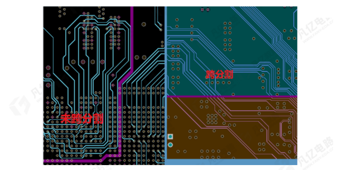
Avoid cross-partition routing for key signal lines
All signal lines on the PCB are impedance-controlled lines with reference planes. Cross-partition routing for key signals must be avoided, as it will cause sudden impedance changes and signal integrity issues. Figure 10 illustrates the phenomenon of signal cross-partitioning.
-
Bus lines with the same function should be routed in parallel with no other signals in between; ground shielding is recommended if space permits;
-
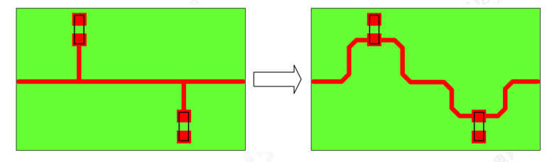
Avoid "U-shaped" or "O-shaped" routing for key signal lines;
-
Do not artificially lengthen key signal lines (route via the shortest path);
-
The distance between key signal lines and board edges/interfaces should be more than 400mil;
-
No routing on any layer under crystal oscillators;
-
No routing under switching power supplies, especially under inductors or conversion chips;
-
Separate transmit and receive signal lines with no cross-routing.
2. Isolation and Protection Routing
- Signal lines connected to surge suppression components (TVS diodes, varistors) should preferably be routed on the outer layers, with short and thick traces (generally more than 10mil);
- Clear routing for different interfaces with no cross-routing;
- Minimize the trace length from interface lines to connected protection and filter components;
- Interface lines must pass through protection/filter components before connecting to signal receiving chips;
- Fixing holes of interface devices should be connected to the protective ground; positioning holes and wrenches connected to the enclosure should be directly connected to the signal ground;
- Separate the input and output grounds of devices such as transformers and optocouplers (use different GND for both ends).
3. Clock Routing
- Clock lines longer than 1 inch should preferably be routed on inner layers with three-dimensional ground shielding;
- Add ground return vias when clock lines switch layers to different ground reference planes;
- Clock lines are not allowed to cross partitions;
- The spacing between clock lines and other signal lines should meet the 5W rule; ground shielding is recommended if space permits;
- Widen or pour copper for the power supply traces of clock circuits.
4. Other Routing Requirements
-
The spacing between protective ground and signal ground should be more than 80mil;
-
Verify that the creepage distance for DC48V is more than 80mil;
-
The power plane should be recessed by 20H relative to the ground plane (H = distance between power and ground planes). Generally, the ground plane is recessed by 20mil, the power plane by 60mil, and ground vias are placed at 150mil intervals;
-
Avoid stub lines in routing (stub lines refer to unused traces or stray paths that signals are not intended to pass through);
 About Maxipcb
Maxipcb empowers innovators to turn cutting-edge technologies into reality.
We offer one-stop solutions for design, simulation, testing, PCB manufacturing, component procurement and SMT assembly, enabling efficient development, rapid deployment and risk control across the full product lifecycle.Serving the world in communications, industrial automation, aerospace, automotive, semiconductor and beyond, we build a safer, more connected future together.
-
The minimum creepage distance for AC220V is 300mil (refer to the creepage distance specification table for details);
-
Differential routing can suppress common-mode interference;
-
Sensitive signal lines must use ground shielding, with GND vias added to the shielding ground every 200mil.


