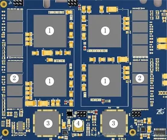
1 Layout Principles
-
Follow the principle of
"Large and critical first, small and simple later": prioritize the layout of important unit circuits and core components.
-
Refer to the functional block diagram during layout and arrange main components according to the main signal flow of the single board. The layout should meet the following requirements as much as possible: minimize the total wiring length, especially for key signal lines; place decoupling capacitors as close as possible to the power pins of ICs to form the shortest loop with the power supply and ground; avoid unnecessary signal traces to prevent signal anomalies.
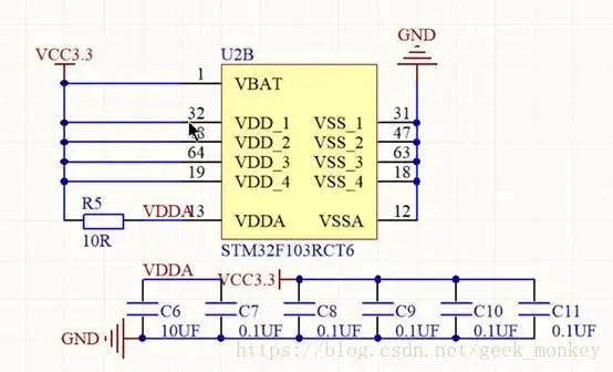
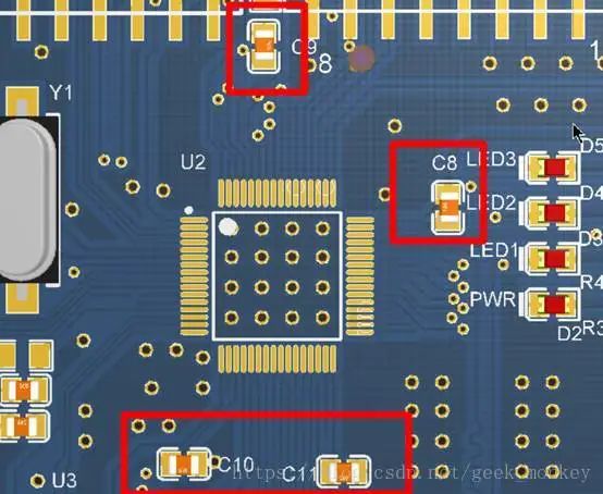
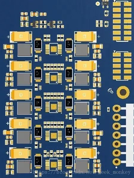
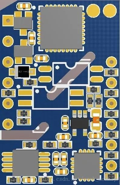
For example, in the diagram below, C8 to C11 are all decoupling capacitors between VCC and GND—their position requirements cannot be reflected in the schematic. However, in PCB design, they should be placed near the power input pins of the chip (e.g., capacitors near pins 31 & 32, and pins 18 & 19).

-
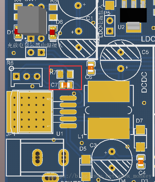
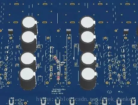
Arrange components for easy debugging and maintenance: do not place large components around small ones, and leave sufficient space around adjustable components—overcrowding will cause operational inconvenience. As shown in the diagram below for R7 and C7, soldering R7 and C7 will be difficult if surrounding components are soldered first (this also indicates the importance of soldering sequence).
-
For circuit parts with the same structure, adopt a
symmetrical standard layout as much as possible; optimize the layout based on uniform distribution, center of gravity balance, and neat board appearance.
-
Mounted components of the same type should be placed in the same direction along the X or Y axis. Polarized discrete components of the same type should also be aligned along the X or Y axis to facilitate production and inspection (manual polarity confirmation may increase production costs).
-
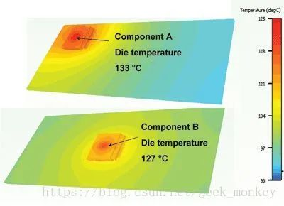
Heat-generating components should be evenly distributed to facilitate heat dissipation of the single board and the whole machine. Temperature-sensitive components (excluding temperature detection components) should be kept away from high-heat components. In addition to temperature sensors, triodes are also heat-sensitive devices.
-
Strictly separate
high-voltage, high-current signals from
low-current, low-voltage weak signals; separate analog signals from digital signals; separate high-frequency signals from low-frequency signals; leave sufficient spacing between high-frequency components. During component layout, try to place devices powered by the same power supply together for convenient subsequent power isolation.
2 Routing Principles
The above are the key considerations for component placement (layout). Routing (interconnection) is relatively more complex, and the general principles are as follows:
- Key signal priority: Prioritize routing critical signals such as analog weak signals, high-speed signals, clock signals and synchronous signals.
- Density priority: Start routing from the components with the most complex connection relationships and the densest wiring areas on the single board.
The core guidelines for routing can be summarized as:
- Allocate dedicated routing layers for key signals (clock, high-frequency, sensitive signals) as much as possible and ensure their minimum loop area. If necessary, adopt manual priority routing, shielding and increased safety spacing to ensure signal quality.
- Avoid routing interference-sensitive signals between power and ground planes, as the EMC environment in this area is poor.
- For networks with impedance control requirements, route strictly in accordance with the specified line length and width.
3 Layout Example Based on Schematic Diagram
Improper layout will lead to inconvenient board use and high routing difficulty.
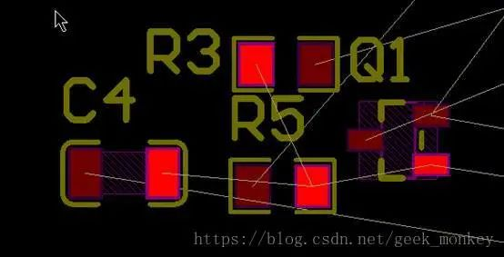
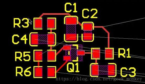
Components that perform a single function should be placed as close together as possible. The operation skills are illustrated with examples below:
- Locate the components of the op-amp module in the schematic and select them by holding the Ctrl key.
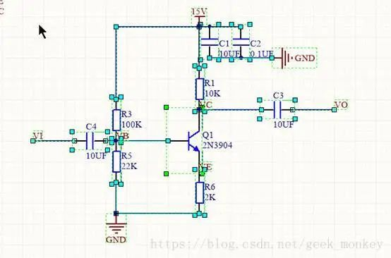
- The selected components will be automatically highlighted in the PCB design interface.
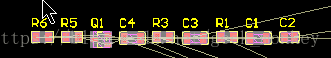
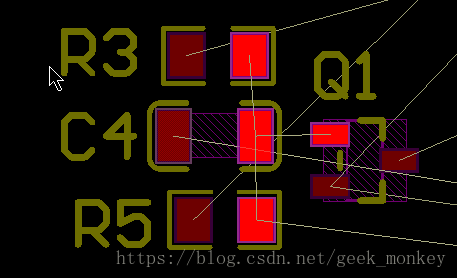
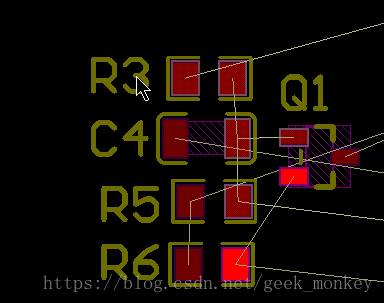
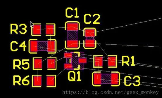
- Check the connection relationships in the schematic (e.g., C4 is connected to R3, R5 and Q1), and place these components close together in the PCB.
- Check the pre-routing traces; select a pad with the VB network attribute by holding the Ctrl key to highlight all VB-related traces for easy layout adjustment.
- Adjust the layout of connected components in turn (e.g., drag R6 close to Q1 as Q1 is connected to R6 in the schematic).
- Complete the routing after the optimal layout is confirmed—this will make the routing process smooth and efficient.
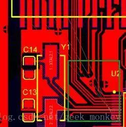
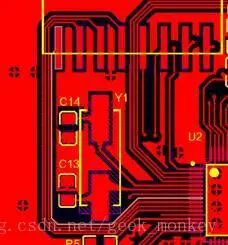
4 Routing Example for Low-Frequency Double-Sided PCBs
Take a PCB with a reset circuit and a sensor expansion interface as an example:
After importing components into the PCB, complete the layout according to the above principles first, then follow these routing steps:
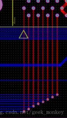
- Route signal and clock lines first: Minimize the length of signal lines (UART, 485, CAN) and reduce vias as much as possible; match the length of differential signals if required. Clock lines (e.g., crystal oscillator signals) should also be short with few vias.
- Route power lines next: For multiple power supplies (e.g., VCC and VCC3.3), set dedicated width rules for power lines. Minimize vias for power lines; if vias are necessary, use multiple parallel vias.
- Route ground lines (or pour copper): Large-area copper pouring is recommended instead of separate ground lines if possible. If ground lines are required, follow the width rule:
Ground line > Power line > Signal line
- Route other lines: Before routing, plan to arrange horizontal lines and vertical lines on different layers in the same area to avoid unnecessary crossings.

- Appropriate adjust component orientation to facilitate routing; keep lines with the same destination neat and use the interactive multi-wire routing tool for efficient operation.
If line crossings are unavoidable, route around a large loop (consider signal attributes when doing so).
 About Maxipcb
Maxipcb empowers innovators to turn cutting-edge technologies into reality.
We offer one-stop solutions for design, simulation, testing, PCB manufacturing, component procurement and SMT assembly, enabling efficient development, rapid deployment and risk control across the full product lifecycle.Serving the world in communications, industrial automation, aerospace, automotive, semiconductor and beyond, we build a safer, more connected future together.


