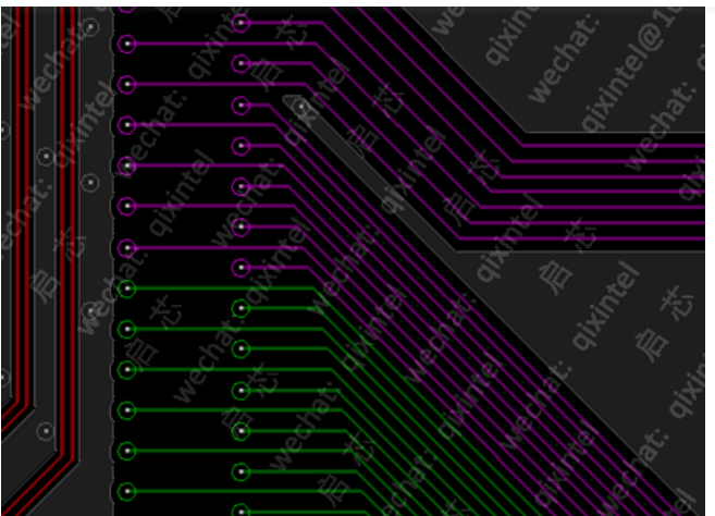
After reviewing numerous PCB designs from colleagues and customers, a common issue is identified: hardware engineers often place a row of vias that disrupt the GND plane, as illustrated in the following figures.
After reviewing numerous PCB designs from colleagues and customers, a common issue is identified: hardware engineers often place a row of vias that disrupt the GND plane, as illustrated in the following figures.
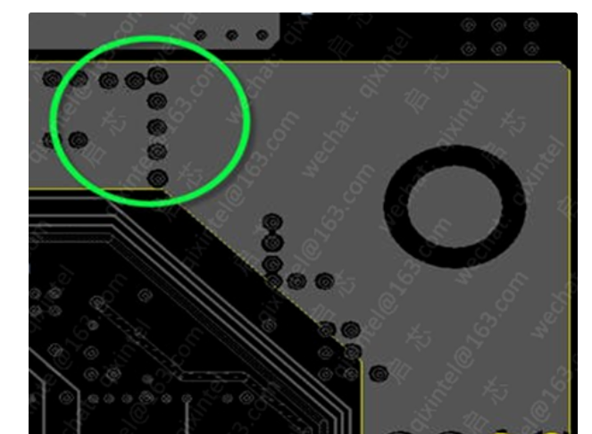
The key issue in this figure is a current bottleneck caused by five vertically aligned vias, which fails to meet current-carrying requirements.
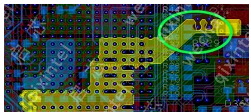
The power plane is segmented by vias, creating a current bottleneck that requires reinforcement.
A row of vias isolates the power plane, resulting in a copper bottleneck that demands reinforcement.
The design specifies a 2A current for this net; however, the copper on one layer is segmented by vias and cannot meet the current-carrying demand, necessitating reinforcement.
Impacts of GND/Power Plane Disruption
- Failure to meet the required current-carrying capacity.
- Lengthened current return paths, leading to increased noise.
A fundamental principle for reducing noise radiation from high-speed signals on PCBs is to minimize the loop area of current return paths. The return current of high-speed signals always follows the path of lowest impedance and shortest distance—typically the GND plane directly adjacent to the high-speed signal trace.
Therefore, placing vias must avoid disrupting the GND plane and creating
ground plane slots. Such slots enlarge the return path area of high-speed signals, increase noise radiation, and cause EMI non-compliance.
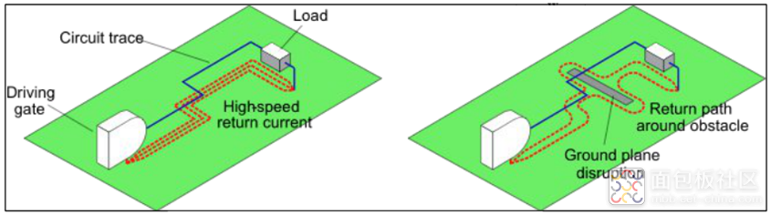

Return current follows the path of least impedance.
If the ground plane/return path is segmented in the RF section:
- Return current paths may become longer.
- Unwanted inductance is added, degrading circuit performance.
It is strongly recommended to avoid disrupting the GND plane with vias, especially for rows of vias in parallel data buses, which create slots that block return paths.
Recommended Solution
Vias should be placed in a staggered arrangement or with adequate spacing. This preserves continuous copper channels in the GND plane to ensure unobstructed return paths for high-speed signals.
Staggered via placement is particularly effective when numerous vias are required. This method maintains sufficient spacing between vias, shortens return paths, and optimizes signal integrity.
About MaxipcbMaxipcb enables advanced electronic innovation. We deliver one-stop solutions including circuit design, simulation, testing, PCB fabrication, component sourcing and SMT&PCBA assembly, to boost R&D efficiency, speed up mass production and control full-cycle risks. We serve global sectors like communication, industrial automation, aerospace, automotive and semiconductor, jointly forging a safer, connected intelligent future.

 The key issue in this figure is a current bottleneck caused by five vertically aligned vias, which fails to meet current-carrying requirements.
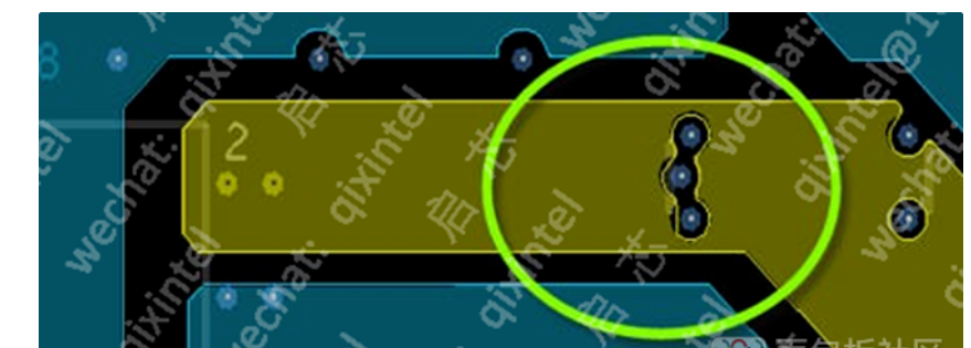
 The power plane is segmented by vias, creating a current bottleneck that requires reinforcement.
 A row of vias isolates the power plane, resulting in a copper bottleneck that demands reinforcement.
 Staggered via placement is particularly effective when numerous vias are required. This method maintains sufficient spacing between vias, shortens return paths, and optimizes signal integrity.