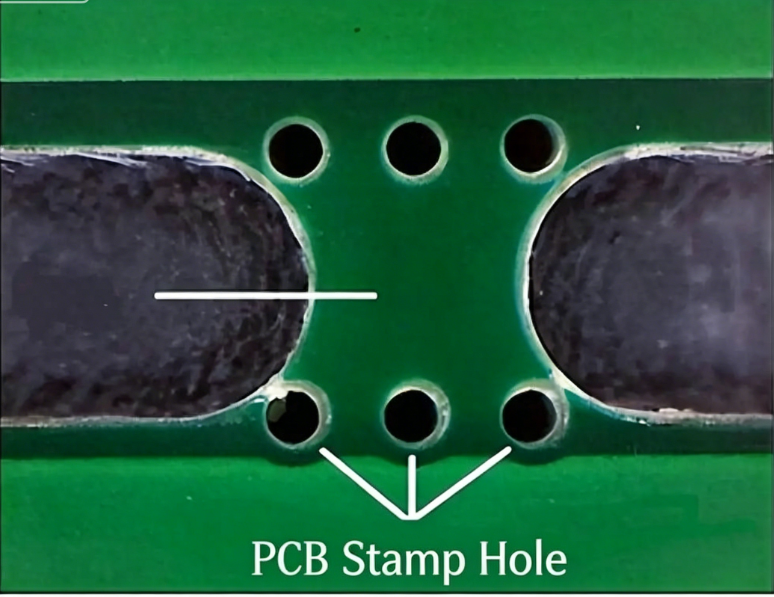
Stamp holes are perforated holes on a mainboard panel used to connect small PCBs arranged in an array, allowing easy removal of individual modules from the PCB assembly.
1. What Are PCB Stamp Holes?
Stamp holes are perforated holes on a mainboard panel used to connect small PCBs arranged in an array, allowing easy removal of individual modules from the PCB assembly.
These perforated structures break cleanly when pressed, enabling component separation
without damaging the PCB itself.
2. Functions of PCB Stamp Holes
PCB stamp holes serve multiple key purposes:
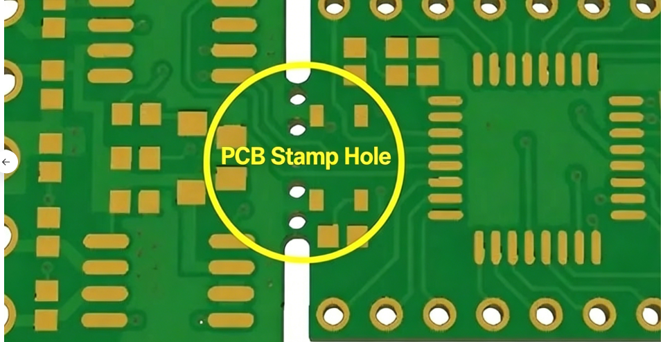
- Grouping small PCBs
When numerous small PCBs require interconnection but are too miniature for standard connectors, stamp holes provide a reliable linking method. The perforated tabs conduct electrical current and connect adjacent PCBs.
- Power and data transmission
Stamp holes enable power delivery and data communication between two distinct PCBs or devices.
3. PCB Stamp Hole Design Requirements
3.1 Number of Stamp Holes
Stamp holes are typically grouped in
sets of 5 for module interconnection, with variations allowed based on specific PCB design needs.
3.2 Stamp Hole Size
The standard diameter of PCB stamp holes is
0.020 inch (0.5 mm), adjustable per PCB design. The hole size is determined by the thickness of the PCB substrate material.
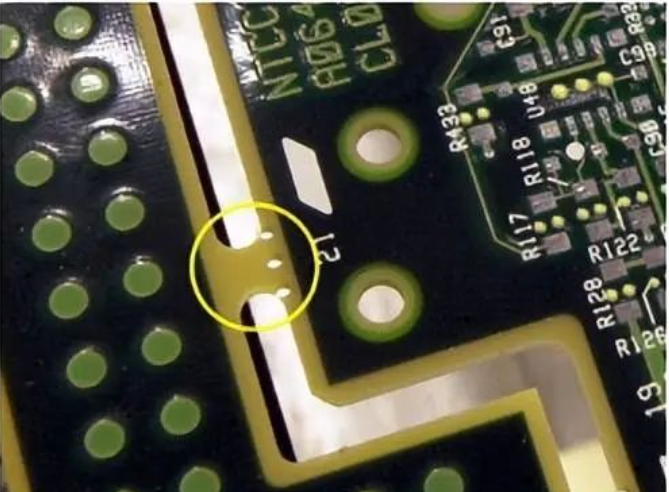
3.3 Stamp Hole Pitch
The standard center-to-center pitch between stamp holes is
0.030 inch (0.76 mm), preventing component overcrowding and short circuits.
4. 4 PCB Stamp Hole Design Tips
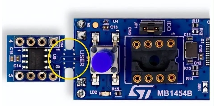
- Use sufficiently robust connecting tabs
Stamp holes create open gaps; weak tabs may break and cause short circuits between PCB sections. Ensure tabs are strong enough to support the weight of mounted components.
- Keep away from sensitive components
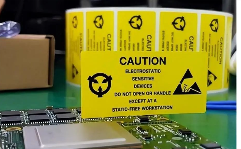
Stamp hole tabs are fragile and prone to damage, which may lead to electrical shorting. They must be placed away from electrostatic-sensitive and other critical components.
-
- Maintain 60 mm–90 mm spacing between stamp hole groups
Excessively large spacing complicates component installation; overly small spacing causes solder migration and short circuits.
- Keep ≥0.125 inch clearance to nearest components
A minimum clearance of 0.125 inch to adjacent components is mandatory, especially for high-density PCBs. Proximity increases soldering difficulty and risks solder bridging between pads and traces.
5. Differences Between PCB Stamp Holes and V-Cuts
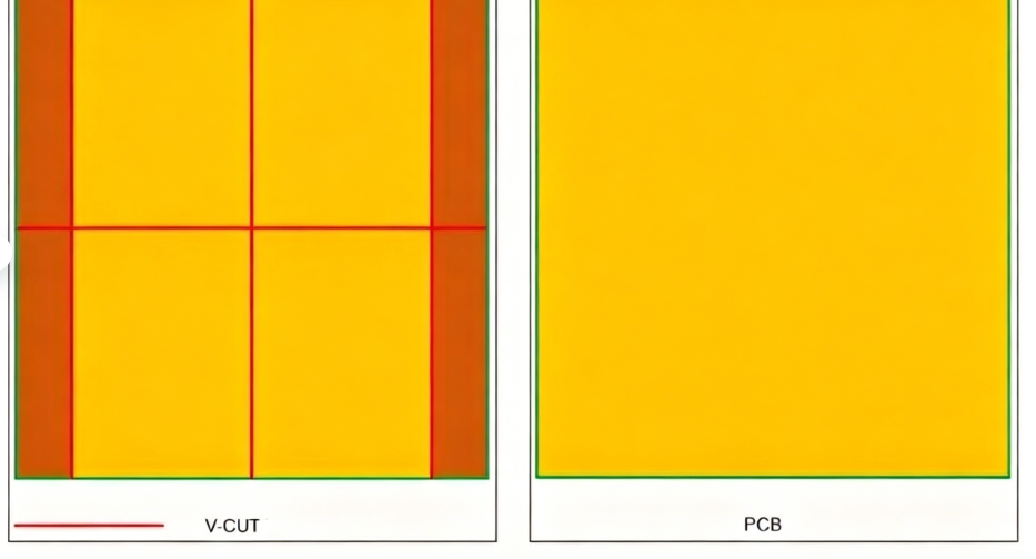
5.1 V-Cut
V-Cut is the most common PCB panelization method. It combines multiple boards or panelized sections, with V-shaped grooves milled by a V-CUT machine after PCB fabrication. The panel breaks easily during use or prior to packaging.
For double-sided V-Cuts, total groove depth (sum of both sides) should be controlled to
approximately 1/3 of the board thickness, with precise dimensions and uniform depth.
Advantages of V-Cut:
- Low cost
- Easier manufacturing
- Better quality and less deformation
5.2 PCB Stamp Holes
Stamp holes are widely used as an alternative to V-Cuts in many designs.
Advantages of Stamp Holes:
- Higher structural strength & direct breakage
No milling equipment is required; the panel breaks cleanly by hand.
- Larger bonding surface area
Larger holes provide greater adhesive grip, simplifying assembly and preventing PCB shifting during processing.
6. IPC-7351 Standards for Stamp Holes
6.1 Preferred Stamp Hole Design (IPC-7351)
Traces must maintain a
minimum clearance of 1 mm from the PCB edge and stamp holes.

6.2 Acceptable Stamp Hole Design (IPC-7351)
Traces on the top edge of the PCB near stamp holes are acceptable if routed correctly with no insufficient spacing, and stamp holes are within IPC-7351 tolerance limits.

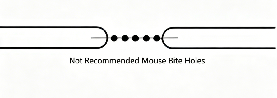
6.3 Non-Recommended Stamp Hole Design (IPC-7351)
Routing traces aligned with the finished board edge or stamp hole tabs is
not recommended, as it may degrade solderability and long-term reliability.
 About Maxipcb
Maxipcb enables advanced electronic innovation. We deliver one-stop solutions including circuit design, simulation, testing, PCB fabrication, component sourcing and SMT&PCBA assembly, to boost R&D efficiency, speed up mass production and control full-cycle risks. We serve global sectors like communication, industrial automation, aerospace, automotive and semiconductor, jointly forging a safer, connected intelligent future.


