Design Rule Check (DRC) rules are constraints defined by engineers based on manufacturing and production standards. All PCB design engineers must comply with these rules to ensure the designed product features normal and reliable functionality and meets mass-production requirements.
1. What Are DRC Rules?
Design Rule Check (DRC) rules are constraints defined by engineers based on manufacturing and production standards. All PCB design engineers must comply with these rules to ensure the designed product features normal and reliable functionality and meets mass-production requirements.
Generally, DRC rules are provided by PCB manufacturers or established internally by companies.
2. Using DRC Rules to Reduce PCB Revision Cycles
DRC rule parameters are critical, and adherence to these parameters helps minimize PCB revision cycles. Nine key parameters are detailed below.
2.1 Minimum Clearance Between Components
The most common DRC parameter is the
minimum clearance between PCB components. Sufficient clearance prevents potential failures such as solder bridging and simplifies assembly, repair, and rework. Larger component clearance eases PCB assembly, while some applications require tight spacing to minimize PCB size.
Special clearance requirements apply to advanced packages, including BGA, POP, large QFP, and QFN:
- IC sockets should be placed as far as possible from sensitive packages. Frequent IC insertion/removal applies excessive stress to adjacent solder joints.
- Sensitive packages should not be placed in the center of the PCB, as board bending and twisting are most severe here and may cause open connections.
- BGAs and other lead-free packages should be placed on only one side of the PCB. If placement on both sides is unavoidable, they must not overlap in the same X/Y position, as this complicates X-ray inspection and rework.
2.2 Clearance From Components to PCB Edge
Component-to-PCB-edge clearance defines the distance from a given component to the board edge. This parameter is critical during
PCB depanelization after assembly.
Components near the PCB edge undergo mechanical stress during depanelization, which risks damaging solder joint integrity.
Clearance requirements for components on the PCB secondary side must be increased, as the solder paste screening process requires a clamping mechanism to prevent PCB movement during paste application.
DRC rules also verify reasonable clearance for trace-to-trace, trace-to-pad, trace-to-via, pad-to-via, and via-to-via spacing to support manufacturability.
2.3 Clearance From Components to Vias
Component-to-via clearance applies to
through-hole technology (THT) components and PCB vias, specifying the minimum distance between component pads and other vias.
Two parameters must be satisfied simultaneously to ensure PCB assembly quality:
- Component to hole wall: Minimum clearance measured from the actual hole edge to the pad edge (standard: 8 mil)
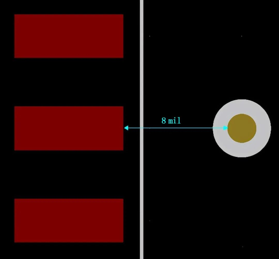
- Component to annular ring: Minimum clearance measured from the annular ring edge to the pad edge (standard: 7 mil)
Detailed separation is required because minimum annular ring size and minimum hole size are non-proportional; both clearance rules must be met during design.
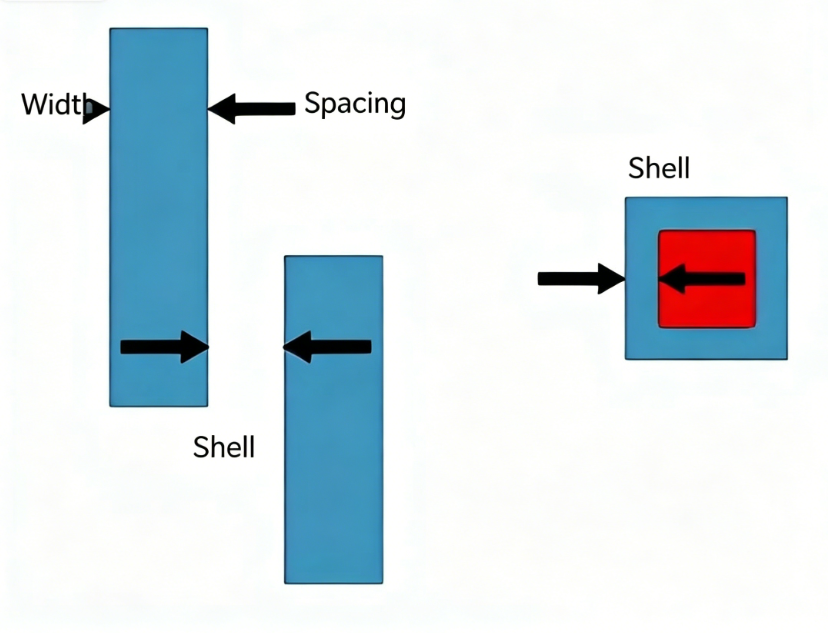
2.4 Minimum Width of VCC and GND Traces
DRC checks validate whether the width of VCC (power) and GND (ground) traces complies with PCB design specifications. They also verify proper tight coupling between VCC and GND and whether GND traces require increased width.
2.5 Minimum Area Requirements
DRC rules specify the overall PCB dimensions and individual component size limits, ensuring compliance with the maximum allowable board area. They also check whether the PCB layout exceeds the defined board outline.
2.6 PCB Silkscreen Placement
DRC checks identify whether silkscreen elements (text, labels, date codes, icons, etc.) cause electrical shortages or other defects. Modifications are required to eliminate risks during subsequent assembly.
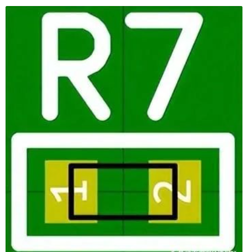
Silkscreen Under Resistors May Cause Reflow Soldering Defects
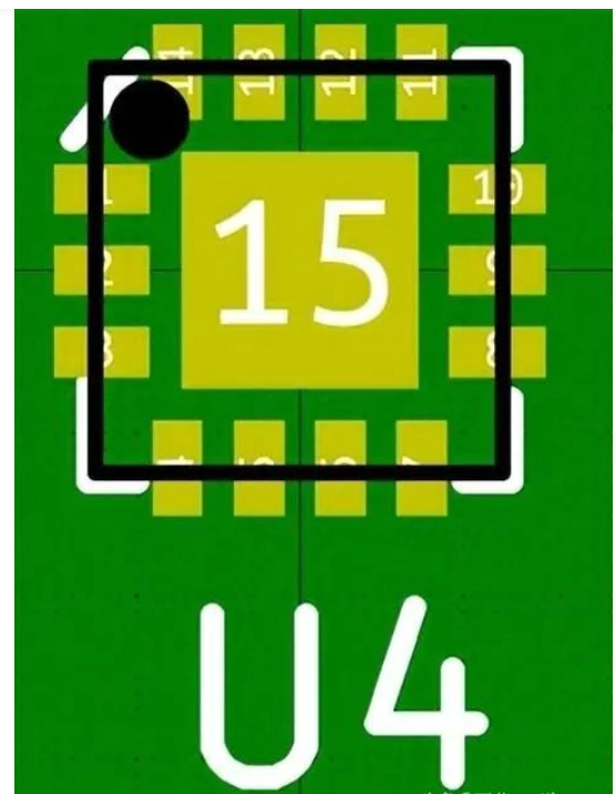
Silkscreen Under QFN Bodies May Cause Soldering Defects and Complicate QFN Rework
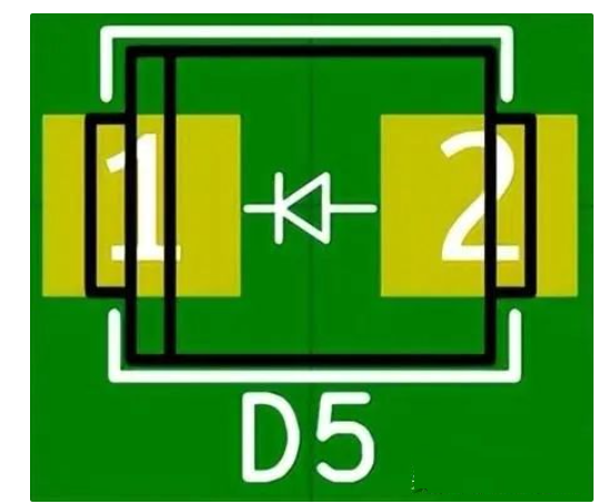
Diode Polarity Markings Obscured After Component Mounting
2.7 Analog and Digital Ground (AGND/DGND)
DRC checks verify that all analog and digital circuits on the PCB use
separate ground connections.
Analog and Digital Ground (AGND/DGND)
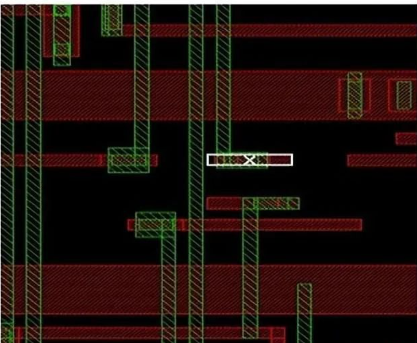
2.8 Via Misalignment
DRC checks confirm aligned via connections between different layers for the same logic network. A via misalignment flag is triggered if vias are misaligned with metal traces during DRC validation.
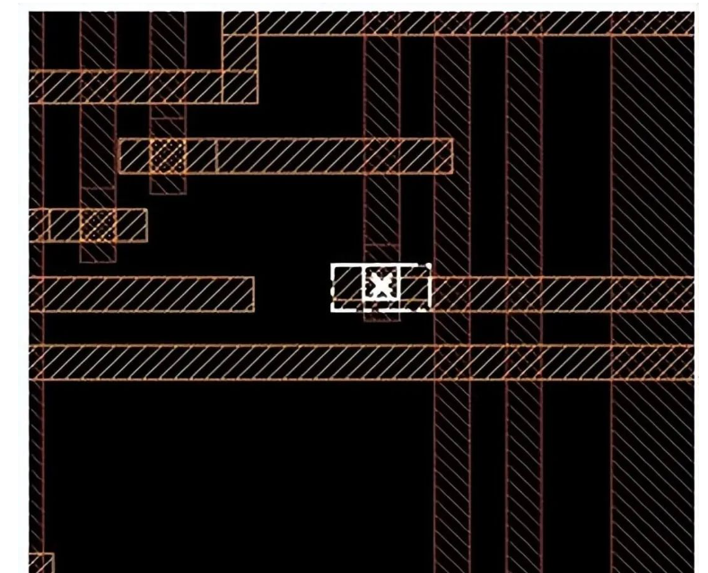
Via Misalignment
2.9 Exposed Power Plane Edges in Multi-Layer PCBs
Another DRC verification parameter is whether the outer edges of power planes in multi-layer PCBs meet ideal standards. Exposed copper on power planes in multi-layer PCBAs poses a high short-circuit risk.
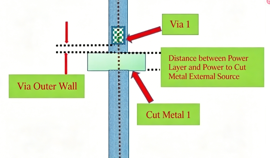
Clearance for Power Plane and Exposed Metal Edges
About Maxipcb
Maxipcb enables advanced electronic innovation. We deliver one-stop solutions including circuit design, simulation, testing, PCB fabrication, component sourcing and SMT&PCBA assembly, to boost R&D efficiency, speed up mass production and control full-cycle risks. We serve global sectors like communication, industrial automation, aerospace, automotive and semiconductor, jointly forging a safer, connected intelligent future.


