In general, when designing ordinary single and double panels, there is no need to consider the stacking problem of PCB, and copper clad laminate with copper thickness and plate thickness meeting the design requirements is usually directly selected for direct processing.
What is PCB stack?In general, when designing ordinary single and double panels, there is no need to consider the stacking problem of PCB, and copper clad laminate with copper thickness and plate thickness meeting the design requirements is usually directly selected for direct processing. However, when designing a PCB with more than 4 layers, the laminated design directly affects the performance and price of the PCB.
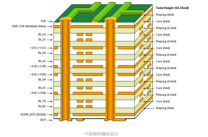
Multi-layer PCB is made of copper-clad Core, prepreg (PP for short) and copper foil, which are combined according to the lamination design and pressed together.
Before PCB design, Layout engineers will determine the number of PCB layers according to the size of the circuit board, the scale of the circuit and the requirements of electromagnetic compatibility (EMC), then determine the layout of components, and finally confirm the division of signal layer, power layer and ground layer.
Design principle of PCB stackPCB stacking needs to be considered from many aspects, such as number of layers, signal type, board thickness, material selection, copper thickness, impedance control, EMI/EMC shielding, thermal management, cost and testability.
Meet the signal integrity requirements of high-speed signal wiring.
For the key signal lines, it is necessary to build a laminated combination of GND/Signal/GND, and the strip lines of adjacent signal layers are crossed vertically to minimize crosstalk coupling. From the point of view of signal integrity, Stripline wiring is used for critical high-speed signals, and Microstrip wiring can be used for non-critical high-speed signals.
If it is not necessary, it is not recommended to use Broadside-Coupled Stripline. The deviation of exposure and etching in PCB processing will cause overlapping and dislocation, and the processing process is difficult and it is difficult to ensure the consistency of impedance.
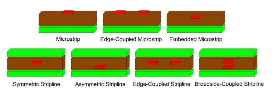
Types of microstrip and stripline wiring
What are the design methods of pcb stack?There are many ways to design PCB stacks. The following are some common ways to design PCB stacks:
For signal layers, each signal layer is usually directly adjacent to the inner electrical layer and effectively isolated from other signal layers to reduce crosstalk. In the design process, multi-layer reference ground plane can be considered to enhance the electromagnetic absorption ability.
In multi-layer board design, such as 10-layer board, there may be different lamination schemes according to the requirements of power supply layer. For example, for the case of a single power layer, one solution is S G S P S G S; For the case that two power layers are needed, the scheme of S G S G P S P S P S can be considered.
In the specific stacking arrangement, increasing the spacing between some layers can control crosstalk, such as increasing the spacing between S1 ~ S2 and S3 ~ S4.
Considering the electromagnetic absorption capacity and power impedance, some stacking methods may have better performance. For example, PCB boards using multi-layer ground reference planes usually have good electromagnetic absorption ability.
The stack design also needs to consider signal integrity, PCB layer to avoid discontinuities and loops, capacitor decoupling and flux elimination, and avoiding unnecessary impedance and loops.
What effect does the stack design have on the circuit?The influence of stack design on the circuit is mainly reflected in the following aspects:
First of all, the laminated design can effectively improve the quality of power supply and reduce crosstalk and electromagnetic interference (EMI). By reasonable stacking layout, such as the signal layer is adjacent to the power layer or stratum, the electromagnetic field distribution can be optimized, the coupling interference between layers can be reduced, and the overall performance of the circuit can be improved.
Secondly, the laminated design helps to save costs. In a limited space, by increasing the number of circuit layers, the integration of the circuit can be improved and more functions can be realized without increasing the PCB area. This is helpful to reduce the size of electronic equipment and meet the trend of miniaturization of modern electronic equipment.
Furthermore, the laminated design can improve the anti-interference ability of the circuit. By introducing insulation layer into the stack, the interference and crosstalk between circuits can be reduced, and the stability and reliability of circuits can be improved. This is especially important for high-speed and high-frequency circuits, which can ensure the accuracy and integrity of signal transmission.
In addition, the laminated design can also reduce the transmission delay of the circuit. Due to the short-distance transmission between circuit layers, the signal transmission time can be greatly reduced, thus improving the working efficiency of the circuit. This is of great significance for applications that need high-speed data transmission.
It should be noted that the stack design also needs to weigh various factors. For example, although increasing the number of circuit layers can improve the integration and performance, it will also increase the manufacturing cost. At the same time, the complexity of laminated design will increase with the increase of layers, which may increase the difficulty of design and manufacture. Therefore, the performance, cost, manufacturing difficulty and other factors need to be considered comprehensively in the design of lamination to find the most suitable lamination scheme.
About Maxipcb
Maxipcb empowers innovators to turn cutting-edge technologies into reality.
We offer one-stop solutions for design, simulation, testing, PCB manufacturing, component procurement and SMT assembly, enabling efficient development, rapid deployment and risk control across the full product lifecycle.Serving the world in communications, industrial automation, aerospace, automotive, semiconductor and beyond, we build a safer, more connected future together.


