There are many key factors to be deeply understood in PCB design, among which the trace width is very important. This aspect is the key to the performance, reliability and optimization of electronic equipment. In this comprehensive guide, we deeply study PCB trace widths and explore their far-reaching influence on signal integrity, thermal management and electrical performance.
There are many key factors to be deeply understood in PCB design, among which the trace width is very important. This aspect is the key to the performance, reliability and optimization of electronic equipment. In this comprehensive guide, we deeply study PCB trace widths and explore their far-reaching influence on signal integrity, thermal management and electrical performance. With knowledge and correct tools (such as PCB trace width calculator), designers can make wise decisions, which will affect the success of their electronic system design. Let's get down to business
What is PCB trace width?PCB trace width refers to the size of the conductive path etched on the PCB substrate to transmit electrical signals between components. It plays a key role in determining the current carrying capacity, impedance and thermal characteristics of the wiring, thus affecting the overall performance and reliability of PCB.
 Key factors affecting the width of wiring:
1. Current carrying capacity:
The main function of PCB wiring is to transmit current from one point to another. The width of the trace directly affects its ability to handle current without exceeding the temperature limit or causing excessive voltage drop.
2. Impedance control:
In high-frequency applications, such as RF (radio frequency) and high-speed digital circuits, maintaining controlled impedance is very important for signal integrity. Trace width, trace spacing and dielectric characteristics will affect the characteristic impedance of transmission lines.
3. Heat dissipation:
PCB traces can also be used as conduits to dissipate heat generated by components or high current. Sufficient trace width is helpful to effectively dissipate heat and prevent thermal problems such as trace delamination or solder joint failure.
4. Voltage drop:
Narrow traces show higher resistance, which leads to an increase in voltage drop along the trace length. By adjusting the trace width, designers can minimize voltage drop and ensure consistent power supply to sensitive components.
5. Manufacturability:
The PCB manufacturing process imposes restrictions on the minimum trace width, which is driven by factors such as copper thickness, etching resolution and manufacturing tolerance. Designers must strike a balance between performance requirements and manufacturability constraints.
Design considerations of trace width:1. Current requirements:
Calculate the maximum current expected to flow through each trace, and determine the appropriate trace width according to the required temperature rise and acceptable voltage drop.
2. Line width calculator:
Use an online trace width calculator or design software tools to estimate the trace width according to current carrying capacity, temperature rise and other parameters.
3. Signal integrity analysis:
Perform signal integrity simulation to ensure controlled impedance and minimize signal attenuation due to reflection, crosstalk or transmission line influence.
4. Thermal management:
Consider the thermal effect of trace width, especially in high power or high density design. The heat is evenly distributed by adjusting the trace width and combining heat holes or heat sinks as needed.
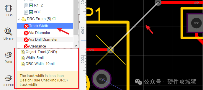
5. Design Rule Check (DRC):
Implement design rule inspection to enforce minimum trace width, gap and spacing requirements to ensure compliance with manufacturing capacity and reliability standards.
 Influence of trace width on electronic system;
1. Performance optimization:
Correct selection of trace width can enhance signal integrity, minimize voltage drop and ensure reliable operation of electronic system, especially in high-speed or high-power applications.
2. Reliability enhancement:
Sufficient trace width can reduce the risk of thermal problems such as trace overheating or solder joint failure, thus improving the long-term reliability and durability of PCB.
3. Manufacturability:
Designing a PCB with optimized trace width can promote a smooth and economical manufacturing process and reduce the possibility of manufacturing errors or production delays.
PCB trace width calculator
By inputting specific parameters such as current load, copper layer thickness, ambient temperature and acceptable temperature rise, these calculators can provide recommended trace width for a given application.
How to calculate the trace width can refer to the following two articles in detail.
Can't set the PCB trace width yet? Formula+case, done in a few minutes.
What is PCB trace width? How to calculate PCB trace width?
Conclusion:The trace width is very important in PCB design, and it is a key factor for the performance and reliability of electronic systems.
About Maxipcb
Maxipcb empowers innovators to turn cutting-edge technologies into reality.
We offer one-stop solutions for design, simulation, testing, PCB manufacturing, component procurement and SMT assembly, enabling efficient development, rapid deployment and risk control across the full product lifecycle.Serving the world in communications, industrial automation, aerospace, automotive, semiconductor and beyond, we build a safer, more connected future together. 


