Multi-layer PCB design requires a method to establish connections between layers, which is achieved through vias ranging from through-hole vias to via-in-pad technology. Traces serve as horizontal connecting elements, while vias act as vertical connecting elements, enabling the transmission of signals and power between board layers.
Multi-layer PCB design requires a method to establish connections between layers, which is achieved through vias ranging from through-hole vias to via-in-pad technology. Traces serve as horizontal connecting elements, while vias act as vertical connecting elements, enabling the transmission of signals and power between board layers.
Before discussing via-in-pad, we first introduce the different types of vias in PCB design.
I. Different Types of Vias in PCB Design
Stacked vias, Staggered vias, Microvias, Through-holes, Blind vias, Buried vias
- Blind vias
Vias connect the outer layer to the inner layers of the PCB without passing through the entire PCB.
- Buried vias
Buried vias connect the inner layers of the PCB, which are more complex and costly to create. These vias originate and terminate in the inner layers of the PCB and are not visible from the outside.
- Microvias
Microvias are tiny holes with a size of 6 mil or less, drilled on the PCB using lasers. Microvias are usually implemented in HDI PCBs.
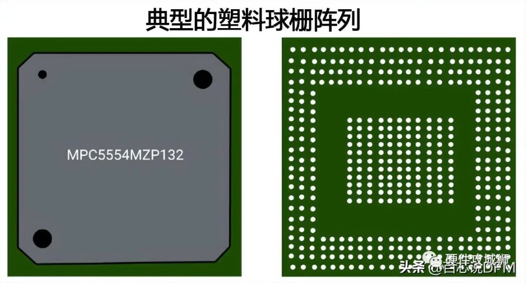
II. What is Via-in-Pad (VIP) Technology?
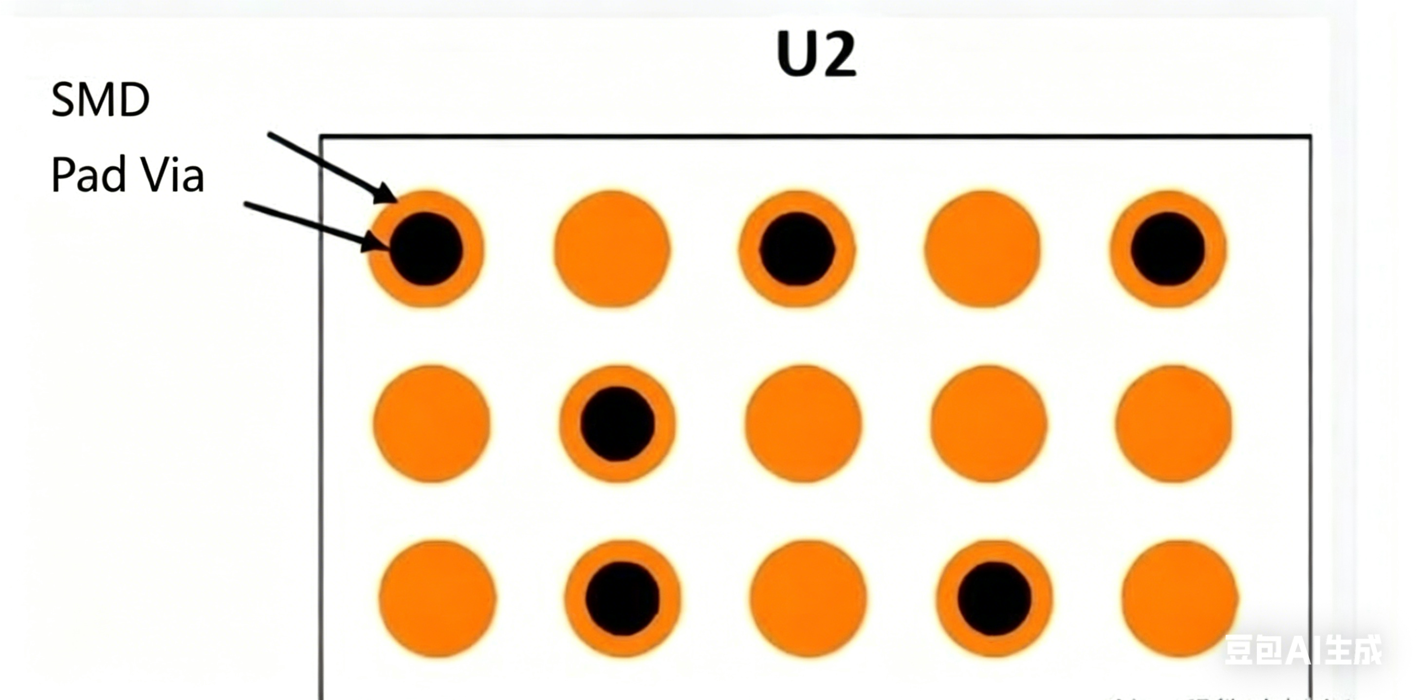
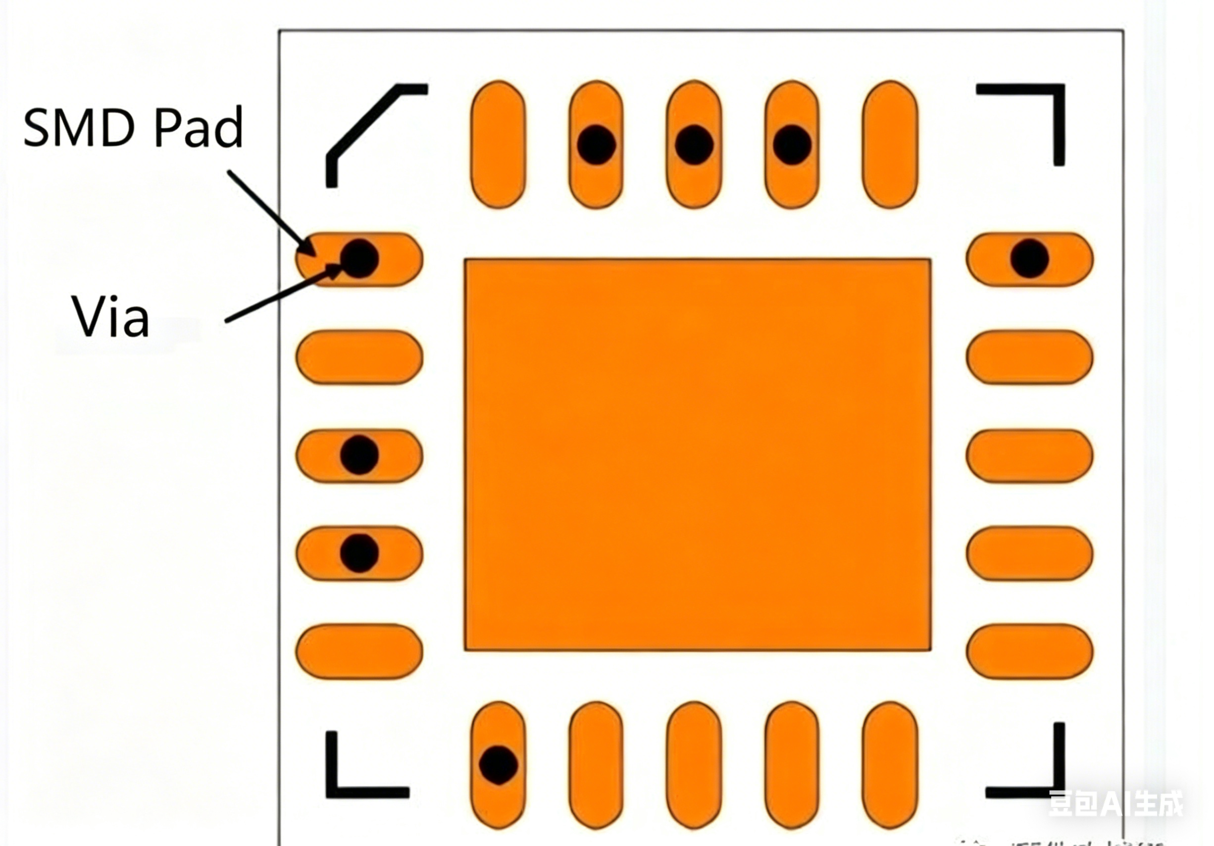
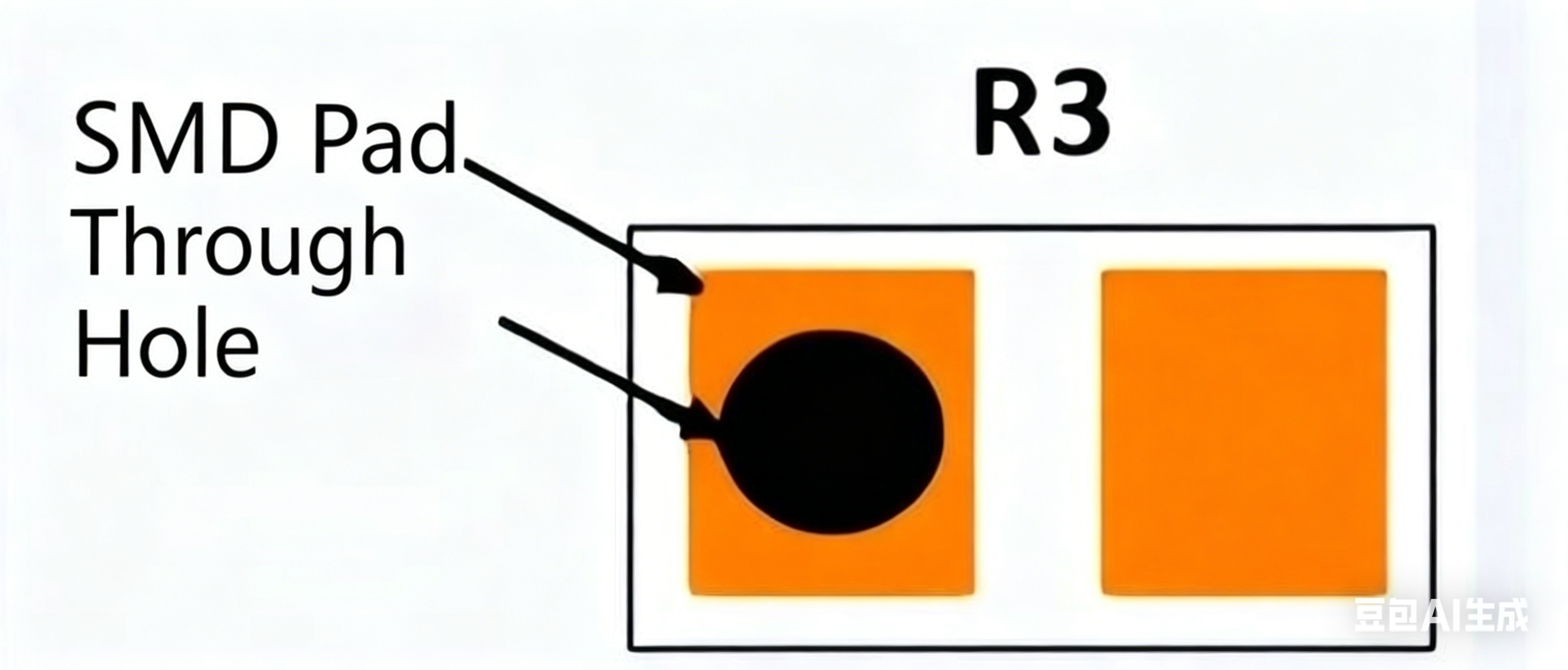
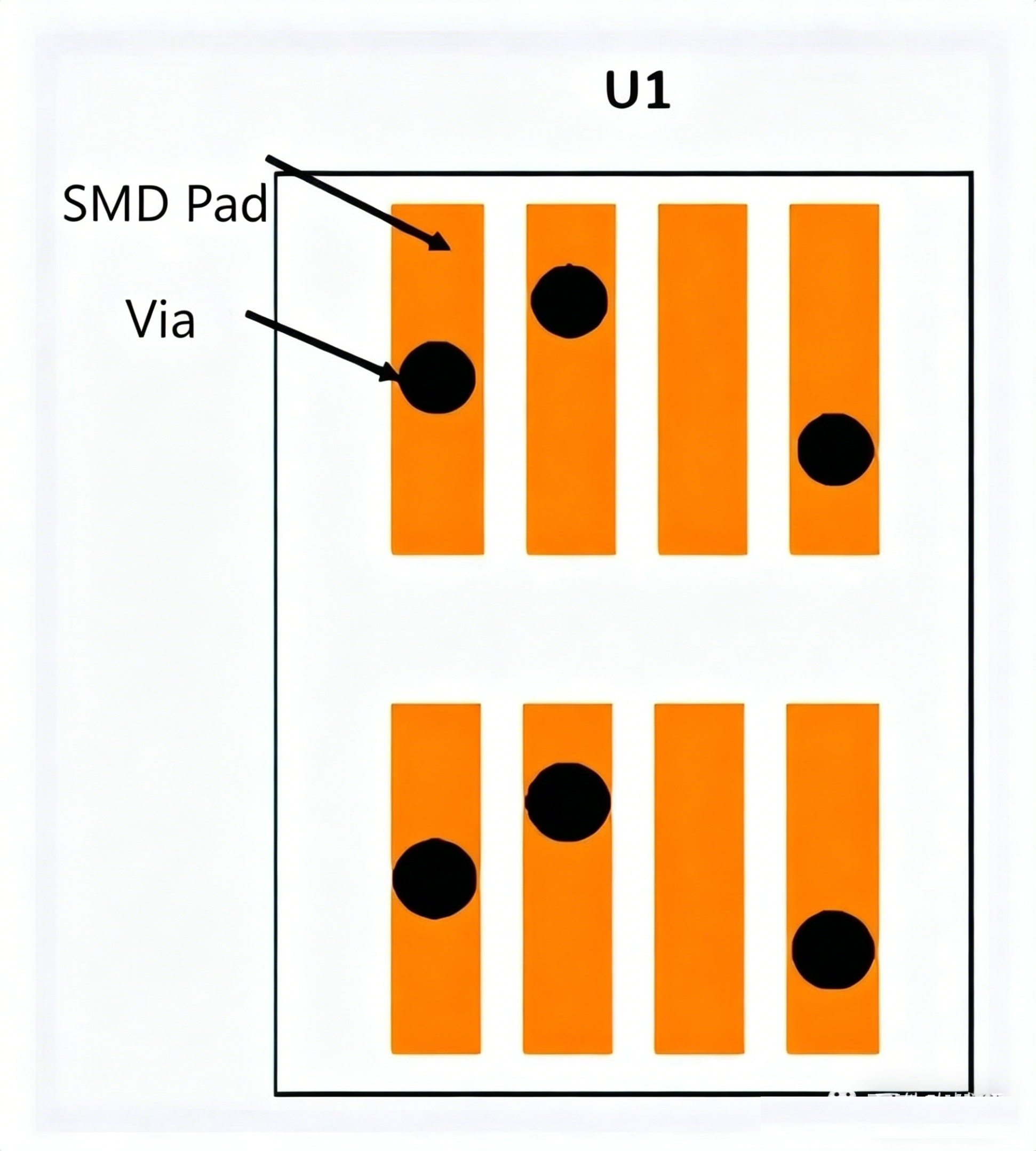
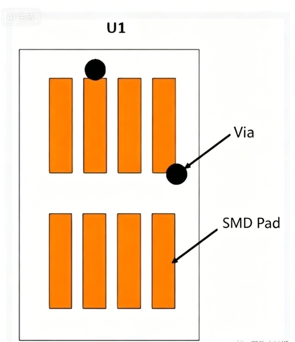
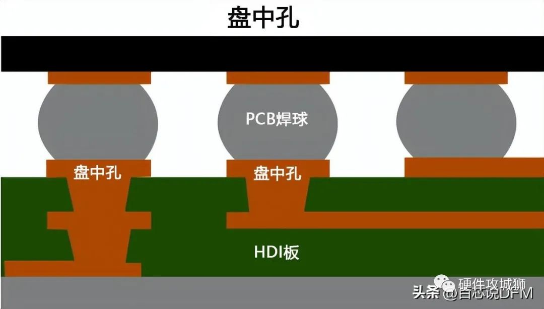
Via-in-pad refers to a via drilled on a pad, where the pad is an SMD pad, usually referring to SMD pads of 0603 and above and BGA pads, commonly abbreviated as VIP (via in pad). The pad of a through-hole component cannot be called a via-in-pad, because the pad of a through-hole component needs to be inserted with component pins for soldering, and all pads of component pins have holes. The following is a schematic diagram of via-in-pad.
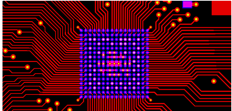
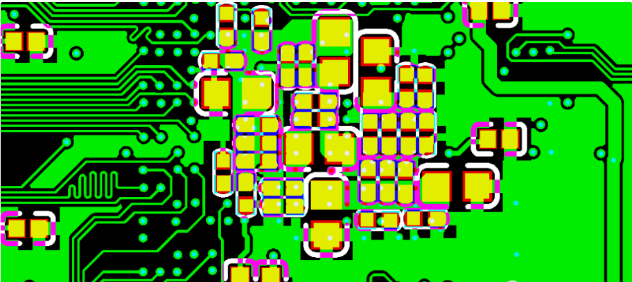
When the pin pitch of a BGA is too small to fan out, the only solution is to drill vias in the pads. In addition, when filter capacitors are placed on the back of a BGA, if the BGA has many pins, the filter capacitors on the back cannot avoid the vias for pin fan-out, and holes have to be drilled on the pads of the filter capacitors.
Therefore, there are two cases of via-in-pad: one is on BGA pads, and the other is on SMD pads. The following figures show various through-holes and via-in-pads in PCB design for clarity.
Via-in-pad is different from traditional vias, in which signal-carrying traces are routed away from the pad to the through-hole. Vias in pads realize the miniaturization of PCB form factor by reducing the space occupied by trace routing. The most typical application of these in-pad vias is for BGA components with a pitch of 0.5 mm or less.
Via-in-pad technology minimizes the signal path length, thereby reducing parasitic inductance and capacitance effects.
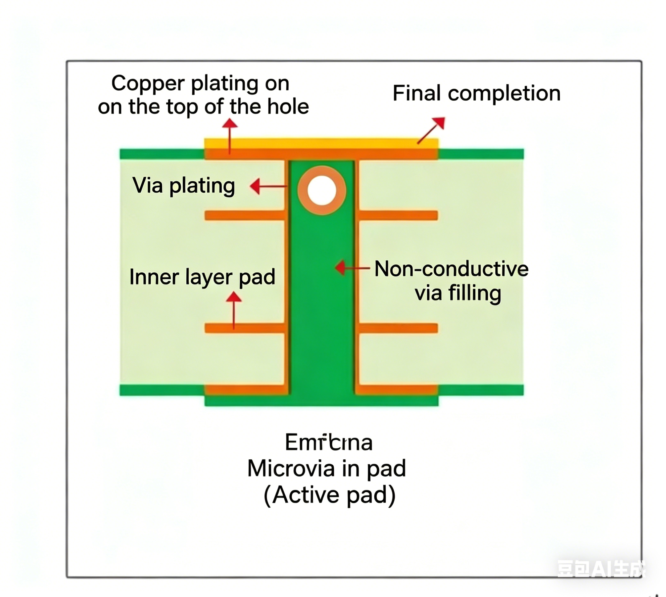
(Copper Plating on the Top of the Hole, Via Electroplating, Non-conductive Via Filling, Final Completion)
III. Design of Via-in-Pad
Here we discuss when via-in-pad needs to be designed and when it does not.
-
No need to design via-in-pad
Fan-out work must be done before PCB routing to facilitate inner-layer routing. For the fan-out of BGA devices, there are too many pins, and the vias for fan-out in the BGA area must be at the center between the pads. Regarding the setting parameters for BGA fan-out: via 0.15-0.2mm, line width 3-4mil, annulus 0.3-0.4mm. Therefore, the BGA pin pitch needs to be greater than 0.35mm for normal fan-out.
-
Need to design via-in-pad
Before BGA fan-out, we need to set the aperture of the via; otherwise, an inappropriate aperture will result in ineffective fan-out or abnormal fan-out results. When the BGA pin pitch is too small to fan out, via-in-pad must be designed for routing from the inner layer or the bottom layer of the BGA device.
-
Via-in-pad on BGA
Generally, devices with few package pins do not require via-in-pad design. BGA devices have many pins, and the vias for fan-out occupy routing space. If the vias are designed as via-in-pad (drilled on the BGA pads), routing space can be reserved. When the pin pitch is too small for routing, via-in-pad is designed for routing from other layers.
-
Via-in-pad on filter capacitors
When many vias need to be drilled for routing inside the BGA device, it is difficult for the filter capacitors placed on the back of the BGA device to avoid the vias. Therefore, vias are drilled on the pads, forming via-in-pad.
IV. Manufacturing Process of Via-in-Pad
- Vias on BGA are generally defined as via-in-pad and need to be filled with resin, and the resin is electroplated with a cap to facilitate customer soldering, unless the customer requires no plugging of the vias on the BGA.
- Except for BGA, when the customer requires all vias to be resin-plugged, the vias on SMD pads are also defined as via-in-pad.
The following are examples of via-in-pad:
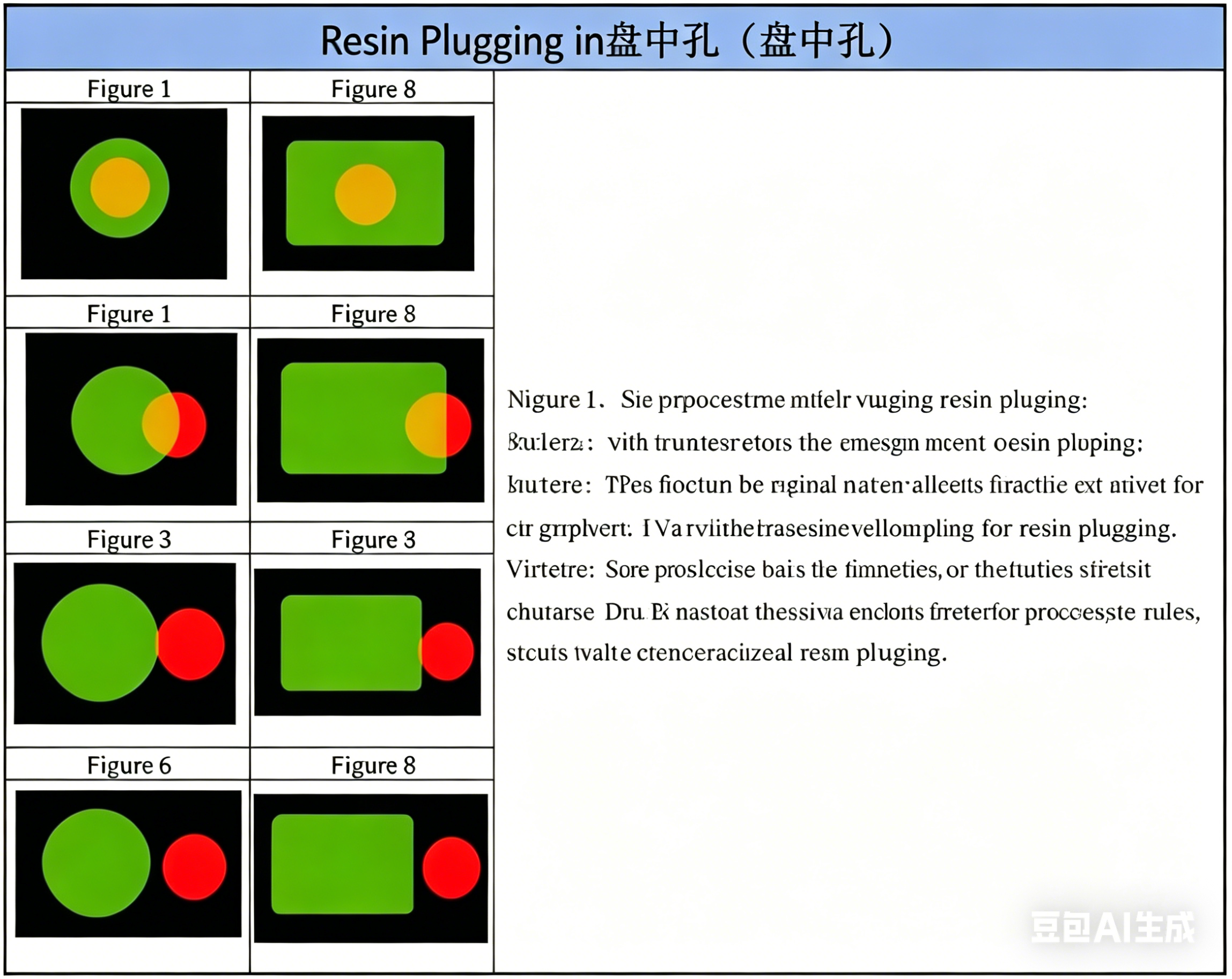
- Figure 1, 5: Standard via-in-pad
- Figure 2, 6: Also belong to via-in-pad
- Figure 3, 7: Vias tangent to the pad (also processed as via-in-pad)
- Figure 4, 8: Vias isolated from the pad (no resin plugging required)
Figures 1, 2, 3, 5, 6, 7 are processed with resin plugging, unless the customer has special requirements.
Manufacturing Process Flow of Via-in-Pad
Drill via-in-pads → Copper plate vias → Fill with resin → Cure → Polish → Reduce copper → Remove excess glue → Drill other non-via-in-pads (usually component holes and tooling holes) → Copper plate vias and VCP surface copper → Normal process...
The following are two examples of processes with and without via-in-pad respectively:
-
Process without via-in-pad
Via-in-pad requires resin plugging, and then the filled resin is copper-plated to facilitate soldering. If the via-in-pad is not processed with the dedicated via-in-pad process and no plugging is done, the result is a small soldering area, and solder balls or resin popping in the holes, leading to cold solder joints.
-
Process with via-in-pad
BGA pads are small, and there is basically no soldering area left if via-in-pad is designed. Therefore, via-in-pad needs to be resin-plugged and the holes filled flat by electroplating to facilitate soldering and avoid poor soldering.
V. Further Design of Via-in-Pad
You can use the solder mask as a blocking medium to prevent solder from being drawn into the through-hole cavity, which is a traditional method. For VIP structures, a completely filled through-hole cavity is required to eliminate trapped air and outgassing, and a precisely flat surface is also required for reliable connection of fine-pitch BGA components.
Manufacturing options available for VIP include mechanical drilling, electroplating and non-conductive epoxy filling methods, as well as laser ablation and full copper-filled via-in-pad methods.
- Non-conductive epoxy via filling
As mentioned above, through-holes in mechanically drilled pads need to be filled with epoxy resin. The selection of epoxy resin largely depends on the coefficient of thermal expansion (CTE) of the via-in-pad filling material and the laminate used. This is important because the filling material will move with or against the surrounding laminate material when the PCB undergoes heating and cooling stages during lamination, which may cause stress-induced fractures and even circuit disconnections.
Non-conductive epoxy resin is a common and cost-effective choice because its CTE is closer to that of the laminate. The PCB design and layout will ultimately determine the type of epoxy resin required for filling the through-holes.
- Creation of via-in-pad
A key feature of the component/device footprint determines the manufacturing method used to create via-in-pad—the pad diameter. To meet the minimum annulus requirements for IPC Class 2 or 3, the pad size should be sufficient to allow for the through-hole diameter and the material dimensions required for manufacturing tolerances.
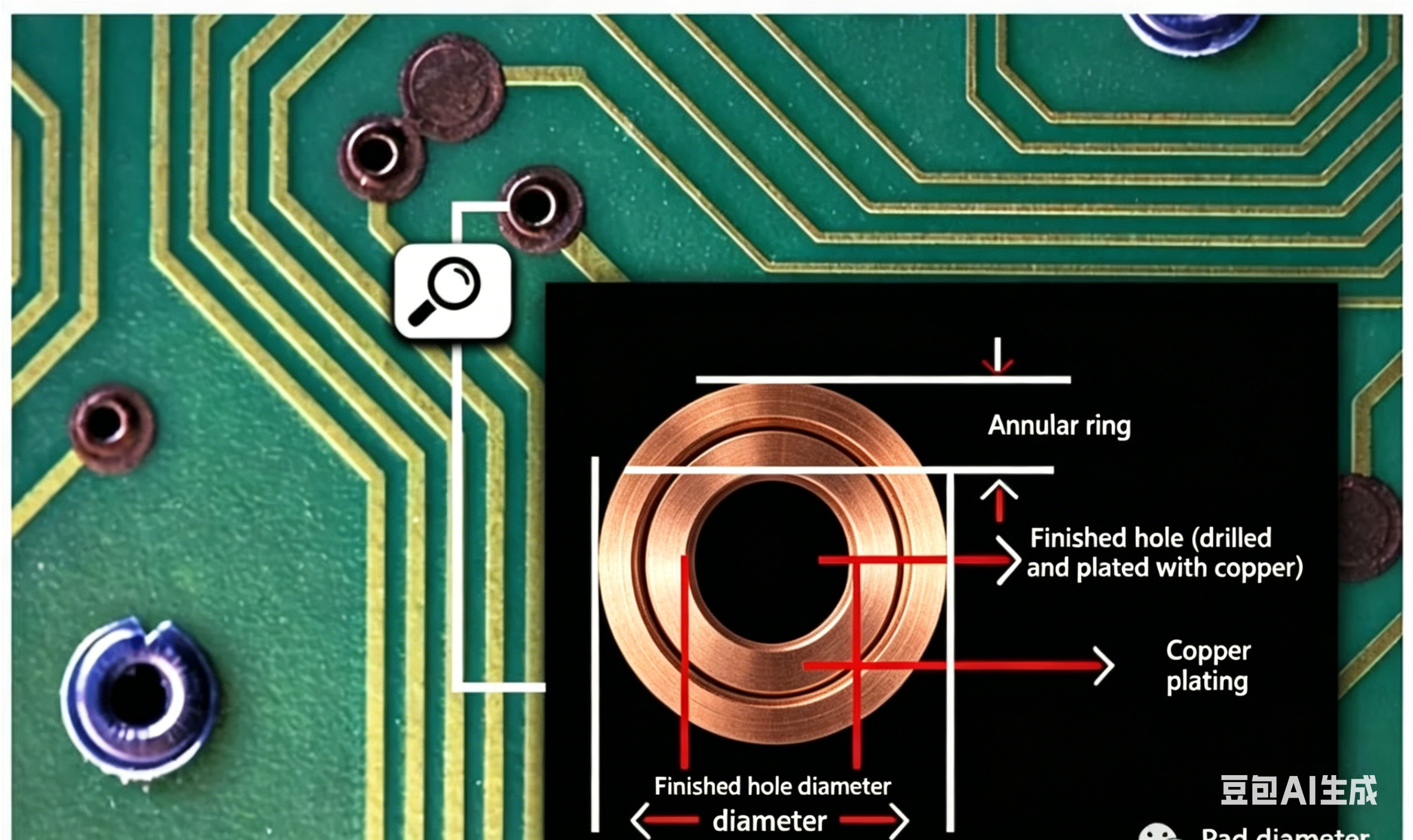
(Finished Aperture, Finished Hole (Drilled and Copper-plated), Copper Plating, Pad Diameter, Annulus)
When using standard mechanical drilling, the pilot drill size (pre-plating drill diameter) and annulus (the pad after drilling and copper plating) need to be considered. When the remaining annulus is insufficient after specifying the minimum drill diameter, laser microvias need to be used. It should be clear that the annulus is the copper pad area around the drilled and finished holes.
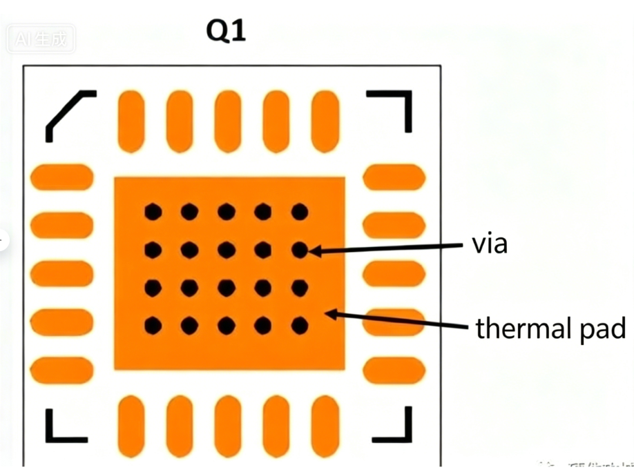
- Common Via-in-Pad Designs
- BGA pad with via-in-pad
- QFN device pad with via-in-pad
- Vias on component pads (e.g., resistors or capacitors)
- Vias in IC pads, connectors or multi-pin components
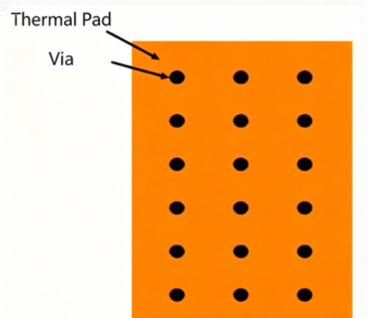
In some cases, via filling is not required. For example, thermal pads do not require soldering, so they are not considered via-in-pad.
- Via-in-Pad without Solder Filling
- Thermal pads without solder filling
- Vias not on pads
Via filling is also not required when vias are not actually placed on pads.
VI. Advantages of Via-in-Pad Routing
Via-in-pad (VIP) routing is used when the circuit board size is limited, the designed components occupy very small space, and surface routing options are limited by the design. Via-in-pad routing is usually used with BGA.
It is also worth noting that when a PCB has complex devices in a compact area, designers place vias in the pads of surface mount devices (SMD) to fan out connections.
PCBs also have other advantages when using VIP routing, compared with other routing options:
- Routing for fine-pitch Ball Grid Array (BGA) is easier, with pitches potentially less than 32 mil and 40 mil (0.8 mm and 1 mm).
- When surface routing is eliminated, bypass capacitors can be placed closer to the components, thereby minimizing inductance, which is useful for enhancing thermal management.
- Since the vias are directly under the components, there is no need for via tenting. Via tenting involves sealing open vias that may draw solder paste during the assembly process.
- Via-in-pad routing is useful for grounding high-frequency components.
VII. Disadvantages of Via-in-Pad Routing
Via-in-pad routing can be implemented by overcoming certain manufacturing complexities, but manufacturers have to eliminate surface protrusions through relatively complex steps, as follows:
- Via-in-pad routing requires the creation and filling of additional through-holes, adding new steps including drilling additional holes and electroplating the through-holes with conductive materials (e.g., copper). The through-holes then need to be filled with epoxy resin and covered with copper.
- Tented vias are sometimes prone to outgassing. Outgassing refers to the release of vapor due to thermal expansion of gas, which is the result of the liquid-to-vapor phase change caused by heating during the lamination process.
- Outgassing causes voids to form in the solder joints as air bubbles move upward through the vias.
VIII. Tips for Via-in-Pad Routing
If the PCB design requires the creation of via-in-pad, you need to reduce manufacturing problems and minimize the additional cost and time required for this specific type of routing. You can use the following via-in-pad guidelines for surface mount device routing:
- Refer to the manufacturer's recommendations for component placement, as well as capping and filling.
- Place microvias on a single layer of the PCB.
- Ensure the non-component side is covered with solder mask.
- Avoid leaving vias open unless necessary—leaving vias open exposes the via copper to the environment, leading to oxidation or corrosion, which shortens the PCB life.
About Maxipcb
Maxipcb empowers innovators to turn cutting-edge technologies into reality.
We offer one-stop solutions for design, simulation, testing, PCB manufacturing, component procurement and SMT assembly, enabling efficient development, rapid deployment and risk control across the full product lifecycle.Serving the world in communications, industrial automation, aerospace, automotive, semiconductor and beyond, we build a safer, more connected future together.


 (Copper Plating on the Top of the Hole, Via Electroplating, Non-conductive Via Filling, Final Completion)


 (Finished Aperture, Finished Hole (Drilled and Copper-plated), Copper Plating, Pad Diameter, Annulus)


