PCB solder mask inks are classified by curing method into photosensitive developing ink, thermosetting ink (cured by heat), and UV-curable ink (cured by UV light). By substrate type, they are divided into solder mask ink for rigid PCBs, solder mask ink for FPC flexible PCBs, and solder mask ink for aluminum substrates (which can also be applied to ceramic substrates).
PCB solder mask inks are classified by curing method into photosensitive developing ink, thermosetting ink (cured by heat), and UV-curable ink (cured by UV light). By substrate type, they are divided into solder mask ink for rigid PCBs, solder mask ink for FPC flexible PCBs, and solder mask ink for aluminum substrates (which can also be applied to ceramic substrates).
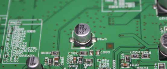
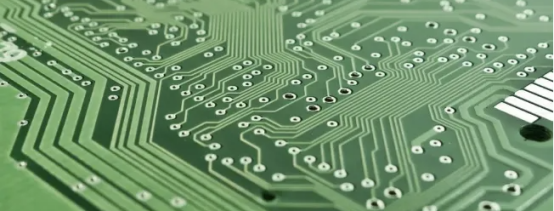
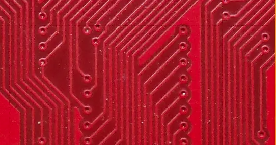
Vias are generally categorized into three types: blind vias, buried vias, and through-holes. Blind vias are located on the top and bottom surfaces of a printed circuit board with a certain depth, used to connect surface and inner-layer circuits. Buried vias are connection holes inside the circuit board and are not visible on the board surface. Through-holes penetrate the entire circuit board, conducting from the top layer through the inner layers to the bottom layer.
Common via processes in the PCB solder mask treatment are: solder mask covered vias, ink-filled vias, solder mask defined vias (open vias), resin-filled vias, and copper paste-filled vias. Each of the five processes has unique characteristics, functions and corresponding application scenarios.
Five Via Treatment Methods and Their Application Scenarios
NO.1 Solder Mask Covered Vias
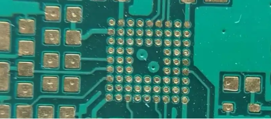
Solder mask covered vias refer to vias whose pads are coated with ink with no tin on the pads, a process adopted for most circuit boards. The aperture of vias designed for solder mask coating is not recommended to exceed 0.5mm; an overly large aperture poses quality risks due to ink accumulation inside the via. When converting PCB design files to Gerber photoplot files for solder mask covered vias, the solder mask opening for vias must be disabled—otherwise, the vias will be processed as open vias instead of covered ones.
NO.2 Solder Mask Defined Vias (Open Vias)
Solder mask defined vias mean the via pads are exposed copper without ink coating, and the surface is finished with immersion gold or hot air solder leveling (HASL) after treatment. The function of open vias is that during wave soldering of components, solder is sprayed onto the inner wall of the vias, which increases the current-carrying capacity of the vias. The effect of open vias is the same as that of through-hole component vias, and there is no need to disable the solder mask opening for vias when converting to Gerber files.
NO.3 Ink-filled Vias
Ink-filled vias refer to vias whose walls are filled with solder mask ink. In production, aluminum sheets are first used to fill the vias with solder mask ink, then the entire board is printed with solder mask ink. The purpose of ink-filled vias is to prevent solder from penetrating through the conductive vias to the component side and causing short circuits during PCB wave soldering. Similarly, the solder mask opening for vias must be disabled when converting design files to Gerber files.
NO.4 Resin-filled Vias
Resin-filled vias refer to vias whose walls are filled with resin, followed by plating to flatten the pads. This process is suitable for all types of vias with a solder mask opening on one side or via-in-pads with openings on both sides. From a process perspective, the purpose of resin filling is to prevent PP adhesive from flowing into the holes during lamination (which would cause adhesive shortage and board popping) for blind and buried vias that are drilled before lamination. From a design perspective, it addresses the issue of insufficient soldering area (which leads to poor soldering) when vias are drilled on pads—if the vias are not filled with resin and plated flat, the soldering area is reduced significantly.
NO.5 Copper Paste-filled Vias
Copper paste-filled vias refer to vias whose walls are filled with copper paste, then plated to flatten the pads. This process is suitable for all types of vias with a solder mask opening on one side or via-in-pads with openings on both sides. The purpose of copper paste filling is to enable via-in-pads to carry high currents. The cost of copper paste-filled vias is much higher than that of resin-filled vias. For design files, simply disable the solder mask opening for vias.
Solder Mask File Design for Vias
01 Via Coating and Opening Settings in Altium
Settings for solder mask opening or coating of vias in Altium software are as shown in the figure: a check mark at the arrow indicates the via is coated with solder mask ink, and no check mark means it is an open via. Vias can be set individually by double-clicking the via and checking the two options as shown in the figure. For bulk setting of solder mask coating (no opening) for all vias, select all vias using the Find Similar Objects function, press F11 to open the PCB Inspector, and check the corresponding options as shown in the figure.
02 Via Coating and Opening Settings in PADS
Settings for solder mask opening or coating of vias in PADS software are as shown in the figure: when converting to Gerber files, click the solder mask layer file, in the pop-up window click Layer, and check the Via option inside for open vias; uncheck it for solder mask covered vias.
03 Via Coating and Opening Settings in Allegro
Settings for solder mask opening or coating of vias in Allegro software are as shown in the figure: when converting to Gerber files, add the VIA CLASS for via solder mask opening in the solder mask layer (add TOP for the top layer and BOTTOM for the bottom layer). Adding the VIA CLASS will result in solder mask defined vias in the Gerber file; not adding it means the vias are coated with solder mask ink.
About Maxipcb
Maxipcb empowers innovators to turn cutting-edge technologies into reality.
We offer one-stop solutions for design, simulation, testing, PCB manufacturing, component procurement and SMT assembly, enabling efficient development, rapid deployment and risk control across the full product lifecycle.Serving the world in communications, industrial automation, aerospace, automotive, semiconductor and beyond, we build a safer, more connected future together.

 Solder mask covered vias refer to vias whose pads are coated with ink with no tin on the pads, a process adopted for most circuit boards. The aperture of vias designed for solder mask coating is not recommended to exceed 0.5mm; an overly large aperture poses quality risks due to ink accumulation inside the via. When converting PCB design files to Gerber photoplot files for solder mask covered vias, the solder mask opening for vias must be disabled—otherwise, the vias will be processed as open vias instead of covered ones.
 Solder mask defined vias mean the via pads are exposed copper without ink coating, and the surface is finished with immersion gold or hot air solder leveling (HASL) after treatment. The function of open vias is that during wave soldering of components, solder is sprayed onto the inner wall of the vias, which increases the current-carrying capacity of the vias. The effect of open vias is the same as that of through-hole component vias, and there is no need to disable the solder mask opening for vias when converting to Gerber files.
 Ink-filled vias refer to vias whose walls are filled with solder mask ink. In production, aluminum sheets are first used to fill the vias with solder mask ink, then the entire board is printed with solder mask ink. The purpose of ink-filled vias is to prevent solder from penetrating through the conductive vias to the component side and causing short circuits during PCB wave soldering. Similarly, the solder mask opening for vias must be disabled when converting design files to Gerber files.
 Resin-filled vias refer to vias whose walls are filled with resin, followed by plating to flatten the pads. This process is suitable for all types of vias with a solder mask opening on one side or via-in-pads with openings on both sides. From a process perspective, the purpose of resin filling is to prevent PP adhesive from flowing into the holes during lamination (which would cause adhesive shortage and board popping) for blind and buried vias that are drilled before lamination. From a design perspective, it addresses the issue of insufficient soldering area (which leads to poor soldering) when vias are drilled on pads—if the vias are not filled with resin and plated flat, the soldering area is reduced significantly.
 Copper paste-filled vias refer to vias whose walls are filled with copper paste, then plated to flatten the pads. This process is suitable for all types of vias with a solder mask opening on one side or via-in-pads with openings on both sides. The purpose of copper paste filling is to enable via-in-pads to carry high currents. The cost of copper paste-filled vias is much higher than that of resin-filled vias. For design files, simply disable the solder mask opening for vias.

