Today's signal processing systems generally need to use mixed-signal devices, such as analog-to-digital converter (ADC), digital-to-analog converter (DAC) and fast signal processor (DSP). In order to process analog signals with wide dynamic range, high-speed and high-performance ADC and DAC signals are more important.
introductionToday's signal processing systems generally need to use mixed-signal devices, such as analog-to-digital converter (ADC), digital-to-analog converter (DAC) and fast signal processor (DSP). In order to process analog signals with wide dynamic range, high-speed and high-performance ADC and DAC signals are more important. In order to maintain the wide dynamic range and low noise of analog signals in the harsh digital environment, it is necessary to use good high-speed circuit design techniques, including proper signal routing, decoupling and grounding.
In the past, "high precision, low speed" circuits were generally regarded as different from so-called "high speed" circuits. For ADC and DAC, the sampling rate (for ADC) and the update rate (for DAC) are used as the criteria to divide the so-called "high speed" and "low speed". However, the following two examples show that most of today's signal processing chips are really "high-speed" chips and must be treated as high-speed devices to maintain their high performance. Such as DSP and AD/DA chips. Sampling adcs (adcs with internal sample-and-hold circuits) for all signal processing applications operate with relatively high-speed clocks. The clock has fast rise and fall times (usually several nanoseconds), so it must be regarded as a high-speed device, even though the conversion rate may be low. For example, a medium-speed 12-bit successive approximation (SAR)ADC works on an internal clock of 10MHz, and the sampling rate is only 500 KSPS. Σ-Δ ADC also needs a high-speed clock, because they have a high oversampling rate.
Even high-resolution, so-called "low-frequency" industrial measurement σ Σ-Δ ADC (with throughput of 10 Hz to 7.5 kHz) operates at a clock frequency of 5MHz or higher to provide 24-bit resolution (for example, AD77xx-series from analog devices). More complicated, mixed-signal IC has both analog and digital ports, so how to use appropriate grounding technology is even more at a loss. In addition, some mixed-signal ics have relatively low digital current, while others have high digital current. In many cases, the two types must be treated differently to achieve the best grounding. Digital and analog design engineers tend to treat mixed-signal devices from different angles. The purpose of this course is to summarize a general grounding principle, which can be used for most mixed-signal devices without knowing the specific details of their internal circuits.
Ground plane and power planeLow impedance and large area ground plane is very important for both analog and digital circuits. The ground plane is not only to provide a low-impedance return path for high-frequency current (generated by high-speed digital logic), but also to minimize EMI/RFI radiation. Due to the shielding effect of the grounding layer, the sensitivity of the circuit to external EMI/RFI is also reduced. The ground plane also allows the transmission line technology (microstrip or stripline) that requires controllable impedance to transmit high-speed digital signals or analog signals. Because "buss wire" has impedance at most logic conversion equivalent frequencies, it is totally unacceptable to use it as "ground". For example, #22 standard wire has an inductance of about 20 nH/ inch. A transient current with a slew rate of 10mA/ns generated by a logic signal will cause a useless voltage drop of 200 mV when flowing through an inch of the conductor at this frequency:
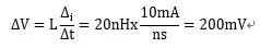
For a signal with a peak-to-peak range of 2 V, this voltage drop will translate into an error of about 10% (about 3.5 bit accuracy). Even in all-digital circuits, this error will lead to a significant decline in the noise margin of logic circuits.
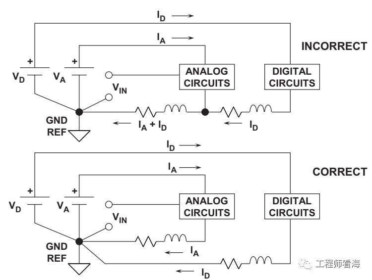 Figure 1: The digital current flowing into the analog return path generates an error voltage.
Figure 1 shows a typical example of digital return current interfering with analog return current (top diagram). The wire inductance and resistance of the grounding path are shared by analog and digital circuits, which will affect each other and eventually produce errors. One possible solution is to let the digital circuit current return path flow directly to GND REF, as shown in the bottom map. This is the basic principle of "star grounding" or single point grounding. It is difficult to realize real single-point grounding in a system with multiple high-frequency return paths, because the physical length of individual current return path leads to parasitic resistance and inductance, which does not conform to the principle of low impedance grounding of high-frequency current. In practice, the current loop must be composed of a large area grounding layer in order to realize low impedance grounding under high frequency current. If there is no low impedance ground plane, it is almost impossible to avoid the above shared impedance, especially at high frequencies.
All integrated circuit grounding pins should be directly connected to the low impedance ground plane, so as to minimize the series inductance and resistance (meaning don't use anything like IC seats). For high-speed devices, it is not recommended to use traditional IC slots. Even in "small size" slots, extra inductance and capacitance may introduce useless shared paths, thus damaging device performance. Individual "pin slots" or "cage sockets" are acceptable if the slots must be used in conjunction with the DIP package, such as during prototyping. The above pin slots are available in both capped and uncovered versions (AMP product models 5-330808-3 and 5-330808-6). Due to the use of spring metal contacts, good electrical and mechanical connection of IC pins is ensured. However, repeated plugging and unplugging may reduce its performance.
Decoupling of low frequency and high frequencyWhen each power supply enters the PC board, it should be decoupled to the low-impedance ground plane through a large-capacity electrolytic capacitor, and the electrolytic capacitor is close to the power supply terminal. This can minimize the low-frequency noise on the power line. In each independent analog stage, each IC package power supply pin needs local filtering only for high frequency (meaning that we commonly use 104 capacitor bypass chip, note that not all cases use 100nF. Use 100nF below 20MHz, and the higher the frequency, the smaller the capacitance).
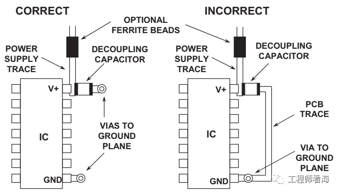
Figure 2: Local high frequency power supply filter provides the best filtering and decoupling through a short low inductance path (ground plane).
Figure 2 shows this method, with the correct implementation on the left and the wrong implementation on the right. In the example on the left, a typical 0.1 μF SMD capacitor is directly connected to the ground plane on the back of PCB through a via, and connected to the GND pin of IC through a second via. In contrast, the setting on the right side is not ideal, which adds extra PCB routing inductance to the grounding path of decoupling capacitor, which reduces the effectiveness. (Conditionally, it is better to put the patch capacitor directly below the back of the chip. )
All high-speed chips (frequency greater than 10MHz) need bypass capacitors similar to those connected in Figure 2 to achieve good performance. Magnetic beads are not 100% necessary here, but they will enhance the isolation and decoupling of high-frequency noise, which is usually beneficial. It may be necessary to verify whether the magnetic beads will be saturated when the IC handles high current. Please note that for some magnetic beads, even before saturation occurs, some magnetic beads may be nonlinear, so if the power stage is required to work with low distortion output, this should be checked and verified.
Double and multilayer PCBEach PCB should have at least one complete layer dedicated to grounding. Ideally, one side of a double-sided circuit board should be completely used for the ground plane and the other side should be used for interconnection. But in practice, this is impossible, because part of the ground plane must be removed for signal and power crossing, vias and vias. Nevertheless, the area should be saved as much as possible, and at least 75% should be kept. After the initial layout is completed, please carefully check the ground plane to ensure that there is no isolated grounding "island" (similar to dead copper), because the IC grounding pin located in the grounding "island" has no current return path to the ground plane. In addition, check whether there is weak connection between adjacent large areas of the grounding layer, otherwise the effectiveness of the grounding layer may be greatly reduced. There is no doubt that automatic wiring technology is generally not suitable for the design of mixed signal circuit boards, so it is strongly recommended that there are a large number of interconnects in the system where manual wiring is integrated by surface mount IC with high density, and multi-layer circuit boards must be used. In this way, at least one whole layer can be dedicated to grounding. A simple 4-layer circuit board has internal grounding and power layers, and the external two layers are used for interconnection of surface mount components. Adjacent to each other, the power layer and the ground layer can provide additional interlayer capacitance (no discrete component can achieve the effect of interlayer capacitance at present), which is helpful for high-frequency decoupling of the power supply. In most systems, four layers are not enough, and other layers are needed for signal and power wiring.
Multi-card mixed signal systemIn the multi-card system, the best way to reduce the grounding impedance is to use the "motherboard" PCB as the interconnection backplane between cards, thus providing a continuous grounding layer for the backplane. At least 30-40% of the pins of PCB connectors should be dedicated to grounding, and these pins should be connected to the grounding layer on the motherboard of the backplane.
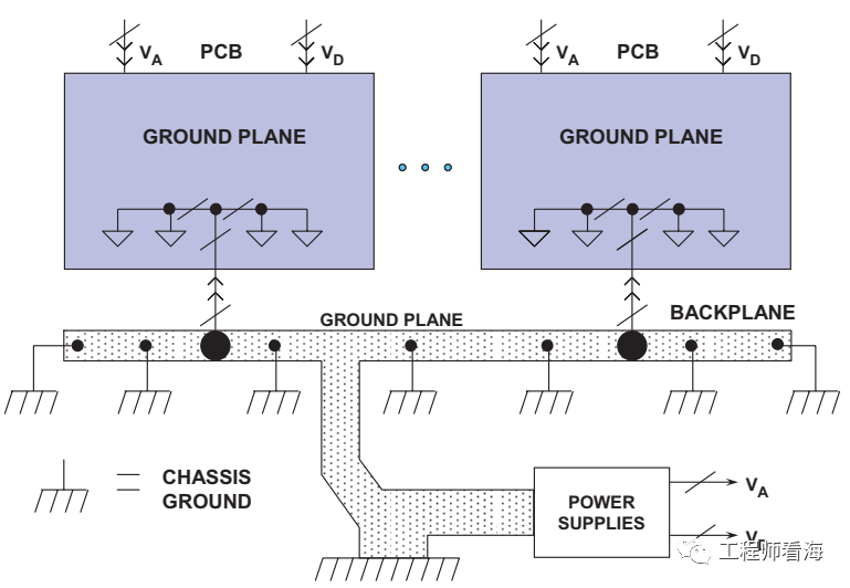 Figure 3: Multi-point grounding concept
Finally, there are two possible ways to realize the overall system grounding scheme: 1. The backplane grounding layer can be connected to the chassis grounding through multiple points, thus diffusing various grounding current return paths. This method is usually called "multipoint" grounding system, as shown in Figure 3. 2. The ground plane can be connected to the "star grounding" point of a single system (usually located in the power supply).
The first method is most commonly used in all-digital systems, but it can be used in mixed-signal systems, provided that the grounding current generated by digital circuits is low enough and spreads over a large area. The PC board, backplane, and chassis all maintain a low resistance path. However, it is very important to make good electrical contact where the ground is connected to the metal plate cabinet. This requires self-tapping screws (that is, the commonly used pointed screws that are tightened more and more every month) and bite washers. Special care must be taken when anodic aluminum oxide is used as the casing material (that is, the casing surface is coated with a layer of aluminum oxide, which is not conductive). At this time, the casing surface is an insulator (meaning this method is not feasible).
The second method ("star grounding") is usually used in high-speed mixed-signal systems with independent analog and digital ground systems, and needs further discussion.
The serial port is composed of analog and digital ground planes.
In mixed-signal systems that use a large number of digital circuits, it is best to physically separate sensitive analog components from noisy digital components. It is also advantageous to use separate ground planes for analog and digital circuits. Avoiding overlap can minimize capacitive coupling between them. Separate analog and digital ground planes continue to extend on the backplane through the motherboard ground plane or "ground net" (consisting of a series of wired interconnections between connector ground pins). As shown in Figure 4, the two layers remain separated until they return to the common system "star" grounding, which is usually located at the power port. The connection between the ground plane, the power supply and the "star" ground should be composed of multiple bus bars or wide copper ribbons to obtain minimum resistance and inductance. Back-to-back Schottky diodes are inserted on each PCB to prevent accidental DC voltage between two grounding systems when inserting and unplugging cards. This voltage should be less than 300 mV to avoid damaging the IC connected to both analog and digital ground planes. Schottky diode is recommended for its low capacitance and low forward voltage drop. Low capacitance can prevent AC coupling between analog and digital ground planes. Schottky diodes begin to conduct at about 300 mV, and if high current is expected, several diodes in parallel may be needed. In some cases, magnetic beads can replace Schottky diodes, but it will introduce DC grounding loop, which will be very troublesome in high-precision systems.
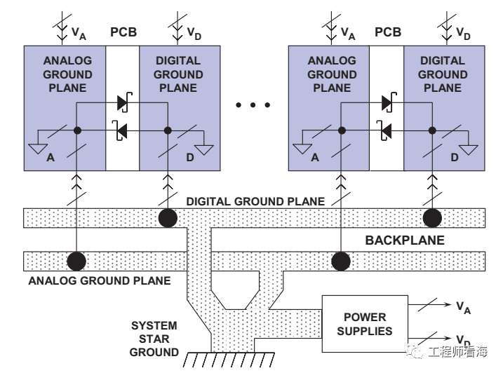 Figure 4: Separate the analog and digital ground planes.
 The ground plane impedance must be as low as possible until it returns to the system star ground. DC or AC voltage higher than 300 mV between two grounding layers will not only damage IC, but also lead to false triggering and possible locking of logic gates.
Grounding and decoupling of mixed-signal IC with low digital currentSensitive analog components such as amplifiers and voltage references are always referenced and decoupled to the analog ground plane. Low digital current ADC and DAC (as well as other mixed-signal IC) should usually be regarded as analog devices, and can also be grounded and decoupled to the analog ground plane. At first glance, this requirement seems contradictory, because the converter has analog and digital interfaces, and usually has pins designated as analog ground (AGND) and digital ground (DGND). The diagram in Figure 5 helps to explain this apparent dilemma.
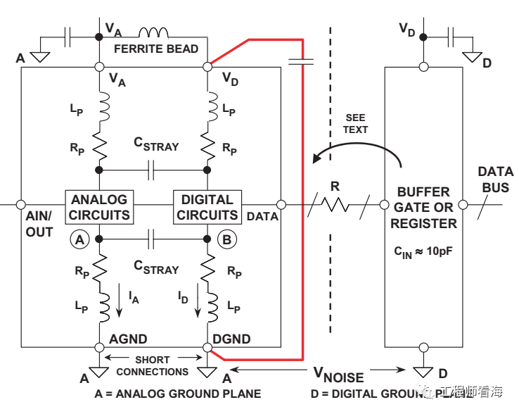 Figure 5: Correct grounding of mixed-signal IC with low internal digital current
Inside an IC (such as ADC or DAC) with both analog and digital circuits, the ground port is usually kept independent to avoid coupling digital signals into the analog circuit. Figure 5 shows a simple converter model. Connecting the chip pad to the package pin will inevitably produce wire bonding inductance and resistance, and IC designers can do nothing about it, as long as they are clear. The rapidly changing digital current generates a voltage at point B, and it is bound to be coupled to point A of the analog circuit through stray capacitor CSTRAY. In addition, there is about 0.2pF stray capacitance between each pin of IC package, which is also inevitable! The task of IC designers is to eliminate this influence and make the chip work normally. However, in order to prevent further coupling, AGND and DGND should be externally connected by the shortest lead and connected to the analog ground plane. Any additional impedance in the DGND connection will generate more digital noise at point B, which in turn will couple more digital noise to the analog circuit through stray capacitance.
Please note that connecting DGND to the digital ground plane will impose VNOISE on both ends of AGND and DGND pins, which will cause serious problems! The name "DGND" on the IC indicates that this pin is connected to the digital ground of the IC, but it does not mean that this pin must be connected to the digital ground of the system. This arrangement may indeed inject a small amount of digital noise into the analog ground plane. However, these currents are very small and can be minimized by ensuring that the converter output does not drive a large fan-out (which is usually not designed).
Minimizing the fan-out on the digital port of the converter can also make the logic conversion of the converter less affected by ringing and reduce the digital switching current as much as possible, thus reducing the possibility of coupling to the analog port of the converter. By inserting small lossy ferrite beads, as shown in Figure 5, the logic power supply pin (VD) can be further isolated from the analog power supply. The internal transient digital current of the converter will flow in a small loop, from VD to DGND via decoupling capacitor (this path is indicated by thick solid line in the figure). Therefore, the transient digital current does not appear on the external analog ground plane, but is confined in the loop. The VD pin decoupling capacitor should be installed as close as possible to the converter to minimize parasitic inductance. These decoupling capacitors should be of low inductance ceramic type, usually between 0.01 μF and 0.1 μF f.
 Handle ADC digital output carefully
It is a good idea to place the buffer register next to the converter (as shown in Figure 5) to isolate the digital line of the converter from the noise on the data bus. Buffer registers also help to minimize the load on the digital output of the converter and provide Faraday shielding between the digital output and the data bus. Although many converters have tri-state output/input, this isolation register still represents a good design method. In some cases, it may be necessary to add additional buffer registers on the analog ground plane next to the converter output to provide better isolation. The series resistance between the ADC output and the input of the buffer register (marked as "R" in Figure 5) helps to minimize the digital transient current, which may affect the converter performance. Resistors can isolate the digital output driver from the capacitance of the buffer register input. In addition, the RC network composed of series resistors and buffer register input capacitors is used as a low-pass filter to slow down fast edges. A typical CMOS gate combined with PCB traces and vias will generate a load of about 10 pF. Without the isolation resistor, a logic output slew rate of 1 V/ns will generate a dynamic current of 10 mA:
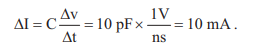
When driving a register input capacitor of 10 pF, a 500 Ω series resistor can minimize this output current and generate a rise and fall time of about 11 ns:

TTL buffer register has a high input capacitance, which can obviously increase the dynamic switching current, so this kind of chip should be avoided. Buffer registers and other digital circuits should be grounded and decoupled to the digital ground plane of the PC board.
Note that any noise between the analog and digital ground planes can reduce the noise margin on the digital interface of the converter. Because the immunity of digital noise is in the hundreds or thousands of millivolts, it is generally unlikely to have problems. The noise of the analog ground plane is usually not high, but if the noise on the digital ground plane (relative to the analog ground plane) exceeds several hundred millivolts, measures should be taken to reduce the impedance of the digital ground plane, so as to keep the digital noise margin at an acceptable level. In any case, the voltage between the two ground planes must not exceed 300 mV, otherwise the IC may be damaged. In addition, it is better to separate the power supply of analog and digital circuits, even if they have the same voltage. The analog power supply should be used to power the converter. If the converter has a specified digital power supply pin (VD), it should be powered by an independent analog power supply or filtered as shown in the figure. All converter power pins should be decoupled to analog ground plane, and all logic circuit power pins should be decoupled to digital ground plane, as shown in Figure 6.
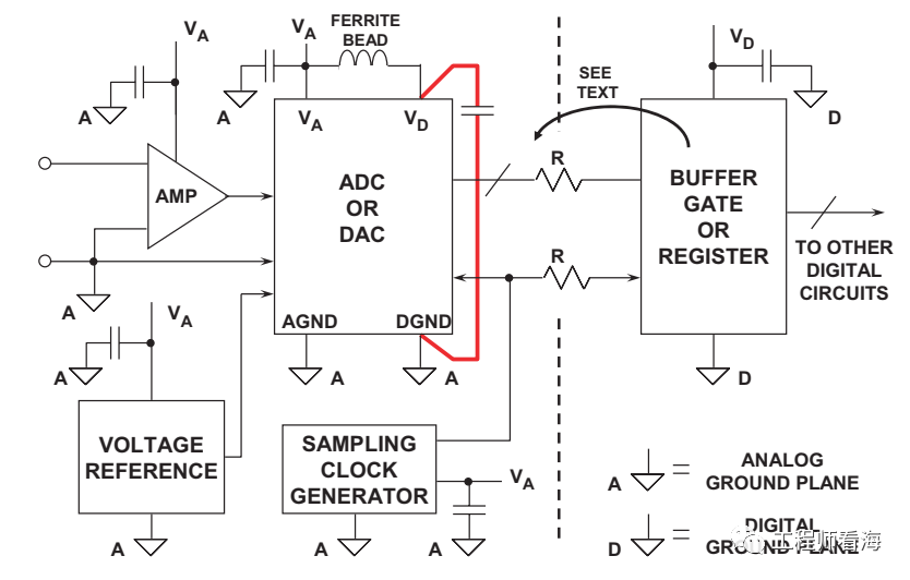 Figure 6: Grounding and decoupling points
In some cases, it is not possible to connect VD to an analog power supply. Some newer high-speed IC may use +5 V power supply for analog circuit and +3 V power supply for digital interface to interface with 3 V logic. In this case, the +3 V pin of the IC should be directly decoupled to the analog ground plane. It is also recommended to connect ferrite beads in series with the power supply trace to connect the pin to the +3 V digital logic power supply. The sampling clock generation circuit should be treated as an analog circuit, and also grounded and deeply decoupled to the analog ground plane. The phase noise on the sampling clock will reduce the system SNR, which will be discussed below.
Precautions for sampling clockIn the high-performance sampling data system, a low-phase noise oscillator should be used to generate the ADC (or DAC) sampling clock. The sampling clock jitter interferes with the analog input/output signal and improves the severity of noise and distortion. The sampling clock generator should be isolated from the noisy digital circuit, grounded and decoupled to the analog ground plane, just like processing operational amplifiers and ADC. The influence of sampling clock jitter on the signal-to-noise ratio (SNR) of ADC can be approximately calculated by the following formula: The only noise source in
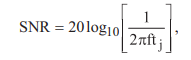
comes from root mean square sampling clock jitter tj. Note that f in the above formula is the analog input frequency. From a simple example, if tj = 50 ps rms and f = 100 kHz, SNR = 90 dB, which is equivalent to a dynamic range of about 15 bits. This effect of clock jitter on SNR is discussed in detail in the course MT-007. However, in most high-performance ADCs, the internal aperture jitter is negligible compared with the jitter on the sampling clock. Ideally, the sampling clock oscillator should refer to the analog ground plane in the separated ground system. However, due to system limitations, this method may not be feasible. In many cases, the sampling clock must be obtained from a higher frequency, multi-purpose system clock generated on the digital ground plane, and then must be transferred from the origin on the digital ground plane to the ADC on the analog ground plane. The ground noise between the two layers is directly added to the clock signal and produces excessive jitter. Jitter can reduce the signal-to-noise ratio and produce interference harmonics.
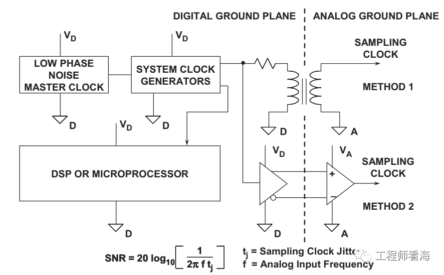 Figure 7: Sampling Clock Distribution from Digital-to-Analog Ground Plane
This problem can be solved to some extent by using a small RF transformer or a high-speed differential driver and receiver IC shown in fig. 7 to transmit a sampling clock signal as a differential signal. Many high-speed ADCs have differential sampling clock inputs, which makes it easier to adopt this method. If active differential drivers and receivers are used, ECL, low level ECL or LVDS should be selected to minimize phase jitter. In a single +5 V power supply system, ECL logic can be connected between ground and +5 V (PECL) power supply, and the output is AC coupled to the ADC sampling clock input. In either case, the original master system clock must be generated from the low phase noise oscillator, not the clock output of DSP, microprocessor or microcontroller. In order to facilitate system clock management, analog devices provides a series of clock generation and distribution products and a complete set of phase locked loop (PLL) solutions.
The origin of mixed signal grounding confusion: applying the concept of single card grounding to multi-card systemMost data sheets of ADC, DAC and other mixed-signal devices discuss grounding for a single PCB, usually the manufacturer's own evaluation board. When these principles are applied to multi-card or multi-ADC/DAC systems, people will feel confused. Generally, it is recommended to divide the grounding layer of PCB into analog layer and digital layer. It is also suggested to connect the AGND and DGND pins of the converter together, and connect the analog ground plane and the digital ground plane at the same point, as shown in Figure 8. In this way, the system "star" grounding is basically generated on the mixed signal device.
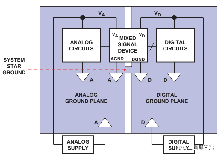 Figure 8: Mixed signal IC grounding: single PC board (typical evaluation/test board)
All high-noise digital current flows into the digital ground plane through the digital power supply and then returns to the digital power supply; Isolated from the sensitive analog part of the circuit board. The star grounding structure of the system appears in the position where the analog and digital grounding layers are connected together in the mixed signal device. This method is generally used in simple systems with a single PCB and a single ADC/DAC, and is usually not suitable for multi-card mixed signal systems. In a system with several ADCs or DACs on different PCBs (or the same PCB as applicable), the analog and digital ground planes are connected at several points, which makes it possible to establish a grounding loop, while a single-point "star" grounding system is impossible. In view of the above reasons, the single-point grounding method is not suitable for multi-card systems, and the above method should be used for mixed-signal IC with low digital current.
Grounding of mixed signal devices with low digital current in multi-card systemFig. 9 summarizes the grounding method of the mixed signal device with low digital current. Since a small digital transient current flows into the small loop between the decoupling capacitors VD and DGND (shown as thick solid lines), the analog ground plane is not damaged. Mixed-signal devices are suitable for all applications as analog components. The noise VN between the ground planes will reduce the noise margin on the digital interface, but if the low impedance digital ground plane is used to keep it below 300 mV and return to the star ground of the system, there is generally no adverse effect.
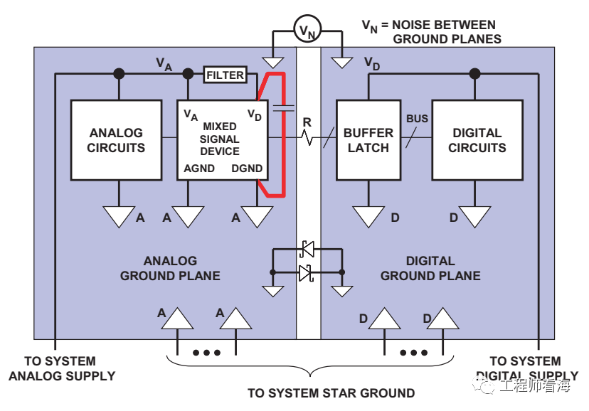 Fig. 9: grounding of mixed-signal IC with low internal digital current: multiple PC boards
However, the digital integration of mixed-signal devices with on-chip analog functions such as σ -δ ADC, codec and DSP is getting higher and higher. Coupled with other digital circuits, the digital current and noise are getting bigger and bigger. For example, σ -δ ADC or DAC contains complex digital filters, which will greatly increase the digital current in the device. The above method relies on the decoupling capacitor between VD and DGND to isolate the digital transient current in a small loop. Here, if the digital current is too large and has DC or low-frequency components, the decoupling capacitor may be too large to be feasible. Any digital current flowing outside the loop between VD and DGND must flow through the analog ground plane. This may degrade performance, especially in high-resolution systems. It is difficult to predict how much digital current will flow through analog ground. At present, we can only recommend alternatives that may have better effects.
Grounding of mixed signal devices with high digital current in multi-card systemAn alternative grounding method suitable for high digital current mixed signal devices is shown in Figure 10. The AGND of the mixed signal device is connected to the analog ground plane, while the DGND is connected to the digital ground plane. The digital current is isolated from the analog ground plane, but the noise between the two ground planes is directly applied between the AGND and DGND pins of the device. In order to successfully implement this method, analog and digital circuits in mixed-signal devices must be fully isolated. The noise between AGND and DGND pins should not be too large, so as not to reduce the internal noise margin or damage the internal analog circuit.
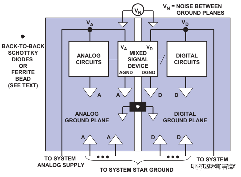 Figure 10: Alternative grounding method for mixed-signal IC with high digital current: multiple PC boards
 As shown in Figure 10, Schottky diodes (back-to-back) or ferrite beads connecting analog and digital ground layers can be selected to connect analog and digital ground. Schottky diode can prevent large DC voltage or low frequency voltage spike at both ends of the two layers. If these voltages exceed 300 mV, the mixed-signal IC may be damaged because they appear directly between the AGND and DGND pins. As an alternative device of back-to-back Schottky diode, ferrite beads can provide DC connection between two layers, but at frequencies higher than several MHz, ferrite beads become resistance, which will lead to isolation. This can protect the IC from the DC voltage between AGND and DGND, but the DC connection provided by ferrite beads may introduce useless DC ground loop, so it may not be suitable for high resolution systems. When the AGND and DGND pins are separated in a special IC with high digital current, try to connect them together if necessary. Through jumper or strip line, you can try two methods to see which one provides the best overall performance of the system.
Grounding summaryNo single grounding method can always guarantee 100% best performance! This section puts forward several possible options according to the characteristics of the specific mixed-signal device under consideration. However, it is helpful to provide as many options as possible when implementing the initial PC board layout. (For example, set up some connection points to test the influence of connection and disconnection on the system during the experiment) At least one layer of PC board must be dedicated to the grounding layer! When the layout of the circuit board is initially drawn, the non-overlapping analog and digital ground planes should be ensured. If necessary, pads and vias should be provided at multiple locations to install back-to-back Schottky diodes or ferrite beads. It is also extremely important to provide pads and vias, and jumpers can be used to connect analog and digital ground planes together when necessary. At present, it is still difficult to predict whether the "multi-point" (single ground plane) or "star" grounding method (separating analog and digital ground planes) can provide the best overall system performance; Therefore, it may be necessary to use jumpers to do some experiments on the final PC board. If you don't feel confident, it's best to separate the analog and digital ground planes first, and then connect them with jumpers later, instead of using a single ground plane at the beginning and then trying to separate them!
Some general PC board layout guidelines for mixed-signal systemsObviously, careful consideration of system layout and prevention of interference between different signals can minimize noise. High-level analog signals should be isolated from low-level analog signals, and both should be far away from digital signals. In the waveform sampling and reconstruction system, we once found that the sampling clock (digital signal) is as susceptible to noise as analog signal, and at the same time it is as prone to noise as digital signal, so it must be isolated from both analog and digital systems. If clock driver packages are used in clock distribution, only one frequency clock should pass through a single package. Sharing drivers between clocks with different frequencies in the same package will cause excessive jitter and crosstalk and reduce performance. Where sensitive signals pass through, the grounding layer can play a shielding role. Figure 11 shows a good layout of the data acquisition circuit board, in which all sensitive areas are isolated from each other and the signal path is as short as possible. Although the actual layout is unlikely to be so neat, the basic principles still apply.
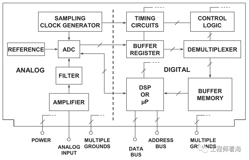 Figure 11: Analog and digital circuits should be separated in PCB layout.
There are many points to consider when performing signal and power connection. First of all, connectors are one of several places where all signal transmission lines in the system must be parallel, so they must be separated from the ground pins (forming Faraday shields) to reduce the coupling between them. There are many points to consider when connecting signals and power supplies. First of all, the connector is one of several positions where all signal transmission lines in the system must be parallel, so they must be separated by grounding pins (forming Faraday shield) to reduce the coupling between them. (To explain this paragraph, the connector refers to something like FPC cable. All signals in these signals are connected in parallel, and defining a ground wire every other signal wire can isolate the interference between signals well.) There is another reason why multiple grounding pins are very important: it can reduce the grounding impedance of the node between the circuit board and the backplane.
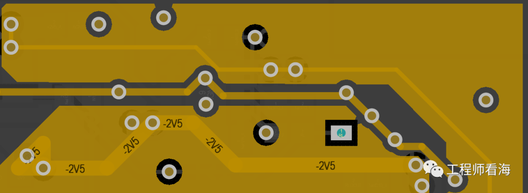
For a new circuit board, the contact resistance of a single pin of PCB connector is very low (10 mΩ level). As the circuit board gets older, the contact resistance may increase and the performance of the circuit board will be affected. Therefore, it is necessary to increase the grounding connection by allocating additional PCB connector pins (about 30 to 40% of all pins on PCB connectors should be grounding pins). For the same reason, each power connection should have several pins, but of course the number need not be as much as the grounding pins. Analog devices and other high-performance mixed-signal IC manufacturers provide evaluation boards to assist customers in initial evaluation and layout. ADC evaluation board generally includes on-chip low jitter sampling clock oscillator, output register and appropriate power supply and signal connector. There are also additional supporting circuits, such as ADC input buffer amplifier and external reference voltage. The evaluation board layout has been optimized for grounding, decoupling and signal paths, and can be used as a model for the layout of ADC PC boards in the system. The actual evaluation board layout is usually provided by ADC manufacturers in the form of computer CAD files (Gerber files). In many cases, the layout of each layer is provided in the device data sheet.
About Maxipcb
Maxipcb empowers innovators to turn cutting-edge technologies into reality.
We offer one-stop solutions for design, simulation, testing, PCB manufacturing, component procurement and SMT assembly, enabling efficient development, rapid deployment and risk control across the full product lifecycle.Serving the world in communications, industrial automation, aerospace, automotive, semiconductor and beyond, we build a safer, more connected future together.


 comes from root mean square sampling clock jitter tj. Note that f in the above formula is the analog input frequency. From a simple example, if tj = 50 ps rms and f = 100 kHz, SNR = 90 dB, which is equivalent to a dynamic range of about 15 bits. This effect of clock jitter on SNR is discussed in detail in the course MT-007. However, in most high-performance ADCs, the internal aperture jitter is negligible compared with the jitter on the sampling clock. Ideally, the sampling clock oscillator should refer to the analog ground plane in the separated ground system. However, due to system limitations, this method may not be feasible. In many cases, the sampling clock must be obtained from a higher frequency, multi-purpose system clock generated on the digital ground plane, and then must be transferred from the origin on the digital ground plane to the ADC on the analog ground plane. The ground noise between the two layers is directly added to the clock signal and produces excessive jitter. Jitter can reduce the signal-to-noise ratio and produce interference harmonics.


