The following summarizes eight formulas, tables and calculation formulas of the relationship between current and line width. Although they are different (generally similar), you can choose an appropriate line width by considering the size of PCB comprehensively in the actual PCB design.
The following summarizes eight formulas, tables and calculation formulas of the relationship between current and line width. Although they are different (generally similar), you can choose an appropriate line width by considering the size of PCB comprehensively in the actual PCB design.
PCB current and line width
The calculation of current-carrying capacity of PCB has always lacked authoritative technical methods and formulas, and experienced CAD engineers can make more accurate judgments by relying on personal experience. But for the novice CAD, it is not a difficult problem.
The current-carrying capacity of PCB depends on the following factors: line width, line thickness (copper foil thickness) and allowable temperature rise. As we all know, the wider the PCB traces, the greater the current carrying capacity. Assuming that under the same conditions, a 10-mil wire can withstand 1A, how much current can a 50-mil wire withstand, is it 5A? The answer is naturally no. Please look at the following data provided by international authorities:
The unit of line width is Inch(1inch=2.54cm=25.4mm).
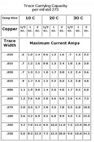
Source: MIL-STD-275 Printed Wiring for Electronic Equipment.
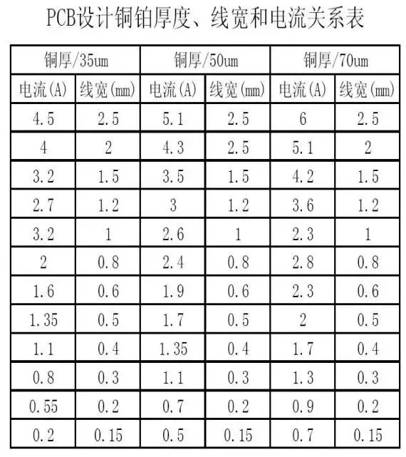
The relationship between copper and platinum thickness, line width and current in PCB design Before understanding the relationship between copper and platinum thickness, line width and current in PCB design, let's understand the conversion between unit ounce, inch and millimeter of PCB copper coating thickness: "In many data tables, the copper coating thickness of PCB is often in ounces, and its conversion relationship with inch and millimeter is as follows:
1 ounce = 0.0014 inch = 0.0356 mm (mm) 2 ounces = 0.0028 inch = 0.0712 mm (mm)
Oz is a unit of weight, which can be converted into millimeters because the copper coating thickness of PCB is "oz/square inch"!
It can also be calculated by empirical formula: 0.15× line width (W)=A, and the above data are all line current carrying values at 25℃.
Conductor impedance: 0.0005×L/W (line length/line width)
In addition, the relationship between the current carrying value of the conductor and the number of vias and pads of the conductor:
There is a direct relationship between the current carrying value of the conductor and the number of vias on the conductor (at present, there is no formula for calculating the influence of pads and via holes per square millimeter on the carrying value of the line, so interested friends can look for it themselves, and I am not sure about it personally, so I don't explain it). Here, I just do some simple main factors that affect the current carrying value of the line.
1. The bearing value listed in the table data is the maximum current bearing value at room temperature of 25 degrees, so various factors such as environment, manufacturing process, plate technology, plate quality and so on should be considered in actual design. So the table is only provided as a reference value.
2. In actual design, each wire will be influenced by pads and vias. For example, the current carrying value of the pad section will be greatly increased after soldering. Perhaps many people have seen a section of wire between pads burned in some high-current boards. The reason is very simple. After soldering, the current carrying value of the pad section is enhanced because of component pins and solder, and the maximum current carrying value of the pad between pads is also increased.
Therefore, when the circuit fluctuates instantaneously, it is easy to burn the line between the pads. The solution: increase the wire width. If the board cannot increase the wire width, add a layer of Solder layer on the wire (generally, you can add a wire with a Solder layer of about 0.6 on a 1mm wire, of course, you can also add a 1mm Solder layer wire). This 1 mm wire can be regarded as a 1.5mm~2mm wire after tin plating.
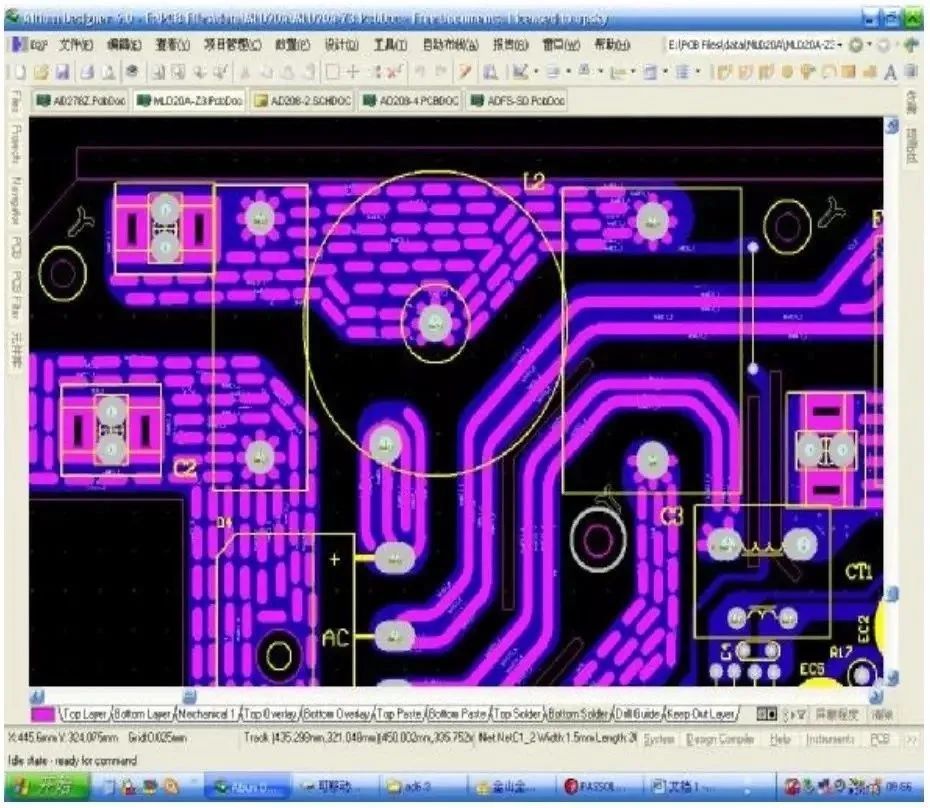
This kind of treatment method is no stranger to those friends who are engaged in PCB Layout of small household appliances, so if the amount of tin is uniform enough and the amount of tin is enough, this 1mm conductor can be regarded as more than a 2mm conductor. This is very important in single-sided high current board.
3. The treatment method around the pad in the figure is also to increase the uniformity of current carrying capacity between the wire and the pad, which is very important especially in the board with large current and thick pins (pins are more than 1.2 and pads are more than 3). Because if the pad is more than 3mm and the pin is more than 1.2, the current of this pad will increase by dozens of times after tin plating. If the current fluctuates greatly at the moment of large current, the current carrying capacity of the whole line will be very uneven (especially when there are many pads), and it is still easy to cause the possibility of circuit burning between pads. Processing like that in the figure can effectively disperse the uniformity of current carrying value between a single pad and peripheral lines.
Finally, it is explained again that the data table of current carrying value is only an absolute reference value, and the design requirements can be absolutely met if the data provided in the table is increased by 10% when the current is not large. In the general single panel design, the copper thickness is 35um, which can basically be designed in the ratio of 1 to 1, that is, the current of 1A can be designed with 1mm wire, which can meet the requirements (calculated at 105 degrees).
The relationship between copper foil thickness, trace width and current in PCB design. When the average current of the signal is large, the current that can be carried by the wiring width should be considered. The line width can refer to the following data:
Relationship between copper foil thickness, trace width and current in PCB design;
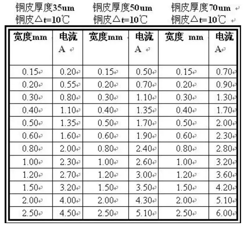
I. When copper skin is used as a conductor to pass a large current, the current carrying capacity of copper foil width should be selected and considered with reference to the numerical derating of 50% in the table.
Ii. In PCB design and processing, OZ (ounces) is commonly used as the unit of copper skin thickness, and 1OZ copper thickness is defined as the weight of copper foil in an area of 1 square foot, and the corresponding physical thickness is 35um;; 2OZ copper is 70um thick.
How to determine the line width of high current conductor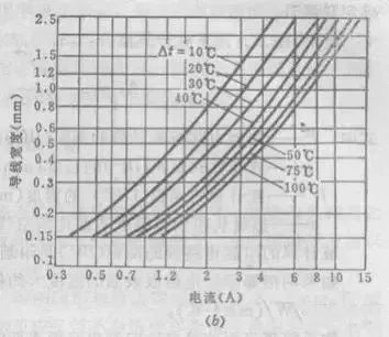
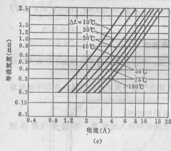
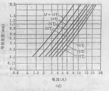
(b) Wire thickness 35μm (c) Wire thickness 70μm (d) Wire thickness 105 μ m.
Calculate (calculate line width, current, impedance, etc.) PCBTEMP by using PCB temperature impedance calculation software.Fill in the Location(External/Internal) conductor on the surface or inside the FR-4 board, Temp temperature (Degree C), Width line width (Mil) and Thickness (Oz/Mil) in turn, and then click Solve to find the passing current, and you can also know the passing current and find the line width, which is very convenient.
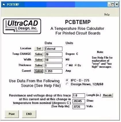
It can be seen that the results of the first method are similar (20 degrees Celsius, 10mil line width, that is, 0.010inch line width, copper foil thickness of 1Oz).
empirical formulaI=KT0.44A0.75K is the correction factor, which is generally 0.024 when the copper-clad wire is in the inner layer and 0.048 when it is in the outer layer;
T is the maximum temperature rise in degrees Celsius (the melting point of copper is 1060℃);
A is the copper-clad cross-sectional area, in square MIL (not mm mm, note that it is square mil);
I is the maximum allowable current in amp.
Generally: 10mil=0.010inch=0.254 can be 1A,
250MIL=6.35mm, which is 8.3A.
The calculation method provided by a netizen is as followsFirst, calculate the cross-sectional area of track. The copper foil thickness of most PCBs is 35um (ask the PCB manufacturer if you are not sure). It is the cross-sectional area multiplied by the line width, and be careful to convert it into square millimeters. There is an empirical value of current density, which is 15~25 amps/mm2. Call it the cross-sectional area to get the flow capacity.
A little experience about line width and copper laying in vias We generally have a common sense when drawing a PCB, that is, use thick lines (for example, 50mil, or even more) for places with high current, and thin lines (for example, 10mil) for signals with low current. For some electromechanical control systems, sometimes the instantaneous current flowing in the wire can reach more than 100A, so the thinner wire will definitely have problems.
A basic empirical value is: 10A/ mm2, that is, the current value that a wire with a cross-sectional area of 1 mm2 can safely pass is 10A. If the line width is too thin, the wiring will burn when a large current passes. Of course, the current burn-out wiring should also follow the energy formula: Q = I * I * T. For example, for a wiring with a current of 10A, a current burr of 100A suddenly appears, and the duration is us-class, then a 30-mil conductor can certainly withstand it. (At this time, there will be another problem, the stray inductance of the wire. This burr will generate a strong back electromotive force under the action of this inductance, which may damage other devices. The thinner and longer the wire, the greater the stray inductance, so it is necessary to consider the length of the wire in practice)
General PCB drawing software often has several options when laying copper on the via pads of device pins: right-angle spokes, 45-degree spokes and straight laying. What's the difference between them? Novices often don't care much, just choose one and be beautiful. In fact, there are two main considerations: first, we must consider not radiating too fast, and second, we must consider the overcurrent capacity.
The method of using direct paving is characterized by the strong overcurrent capacity of the pad, which must be used for the device pins on the high power circuit. At the same time, its thermal conductivity is also very strong. Although it is good for the device to dissipate heat, it is a problem for circuit board welders. Because the pad dissipates heat too quickly, it is not easy to hang tin, so it is often necessary to use a soldering iron with larger wattage and higher welding temperature, which reduces production efficiency. Using right-angle spokes and 45-angle spokes will reduce the contact area between the pin and the copper foil, which will slow down the heat dissipation and make it easier to weld. Therefore, the connection mode of copper laying on via pads should be considered according to the application situation, considering the over-current ability and heat dissipation ability together. For low-power signal lines, direct laying should not be used, but for pads with high current, it must be directly laid. As for the right angle or the 45-degree angle, it depends on the beauty.
Why did you bring this up? Because I have been studying a motor driver for a while, the devices of H-bridge in this driver always burn out, and I can't find the reason for it for four or five years. After some hard work, I finally found out that the pad of a device in the power circuit was paved with right-angle spokes (and because of poor painting, only two spokes actually appeared). This greatly reduces the overcurrent capability of the whole power loop. Although the product has no problems during normal use, it works perfectly under the condition of 10A current. However, when the H-bridge is short-circuited, there will be a current of about 100A in the loop, and these two spokes will burn out instantly (uS level). Then, the power loop becomes an open circuit, and the energy stored in the motor is emitted by all possible means without a drain channel. This energy will burn the current measuring resistor and related operational amplifier devices, destroy the bridge control chip, and rush into the signal and power supply of the digital circuit, causing serious damage to the whole equipment. The whole process is as thrilling as detonating a big mine with a single hair.
So, why are only two spokes used on the pad in the power loop? Why not let the copper foil be laid straight over? Because, the staff in the production department said that it would be too difficult to weld this pin!
About Maxipcb
Maxipcb empowers innovators to turn cutting-edge technologies into reality.
We offer one-stop solutions for design, simulation, testing, PCB manufacturing, component procurement and SMT assembly, enabling efficient development, rapid deployment and risk control across the full product lifecycle.Serving the world in communications, industrial automation, aerospace, automotive, semiconductor and beyond, we build a safer, more connected future together. 


