All traces on a PCB are etched on the copper layers of the stackup. However, routing can rarely be completed on a single layer—except for simple LED boards on aluminum substrates, which carry only current and need no layer changes.
All traces on a PCB are etched on the copper layers of the stackup. However, routing can rarely be completed on a single layer—except for simple LED boards on aluminum substrates, which carry only current and need no layer changes.
The small holes widely seen on PCBs, professionally called
vias, are used to route signals between layers.
Three Typical Via Types
The three most common vias are:
- Through-hole Via
- Blind Via
- Buried Via
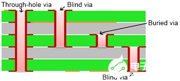
Figure 1 – Diagram of three typical vias: Through‑hole via, Blind via, Buried via
Brief Introduction
- Through‑hole Via: Used in most standard PCBs; connects all layers.
- Blind Via: Used in high‑density layouts (e.g., high‑pin‑count devices, double‑sided mounting). PCBs with blind vias are usually called HDI PCBs (High‑Density Interconnect). Cost is higher than through‑hole vias.
- Buried Via: Very rare; similar to embedded capacitors inside the PCB.
Through‑hole Via Details
A through‑hole via connects traces across all layers.
- Made by mechanical drilling (laser drilling is also available).
- The PCB is fully laminated first, then drilled through all layers.
- Vias are copper‑plated; large circular pads connect traces at signal layers.
- If a via passes through a layer with no connection, a thermal relief/anti‑pad is used to isolate it from copper. Anti‑pads are critical in high‑speed and high‑frequency PCB design.
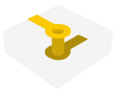
Figure 2 – 3D view of a through‑hole via
BGA Fanout with Vias
Large BGAs and multi‑row connectors require extensive fanout—routing signals to inner layers using nearby vias.
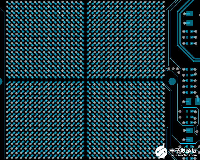
Figure 3 – BGA fanout example with many vias
Common via sizes: 8 mil, 10 mil, 12 mil (based on PCB thickness, aspect ratio, and manufacturing capability).
PCB Design Software Notes
Learning PCB design requires practical skills and professional tools.
Allegro is the industry leading tool:
- Steeper learning curve but highly efficient for daily use.
- Widely used by PCB layout houses.
Other tools: Pads, Altium Designer.
About Maxipcb
Maxipcb empowers innovators to turn cutting-edge technologies into reality.
We offer one-stop solutions for design, simulation, testing, PCB manufacturing, component procurement and SMT assembly, enabling efficient development, rapid deployment and risk control across the full product lifecycle.Serving the world in communications, industrial automation, aerospace, automotive, semiconductor and beyond, we build a safer, more connected future together.


