Switching power supplies are widely used due to high efficiency, wide adjustable output voltage, low loss, small size, and light weight. However, they tend to introduce electromagnetic interference (EMI) issues.
Switching power supplies are widely used due to high efficiency, wide adjustable output voltage, low loss, small size, and light weight. However, they tend to introduce electromagnetic interference (EMI) issues.
1. EMI Classification
EMI is divided into two categories:
- Conducted interference
- Radiated interference
Conducted interference is further split into:
- Differential-mode (DM) interference: below 30 MHz
- Common-mode (CM) interference: 30 MHz–100 MHz
These interferences propagate via wires or common power lines.
- DM interference: suppressed by DM π‑filter
- CM interference: suppressed by CM inductor
This article focuses on low‑frequency DM interference solutions and PCB routing guidelines.
2. Adding Conducted Interference Suppression Components
Conducted interference is easier to mitigate than radiated interference. A π‑filter at the input usually passes low‑frequency conducted tests.
Example Circuit (XL4013)
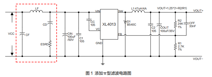
Figure 1 – XL4013 circuit with π‑filter (red box)
Test Comparison
Test conditions: XL4013, VIN=24 V, VOUT=12 V/2 A
- Figure 2: Conducted noise without π‑filter
- Figure 3: Conducted noise with π‑filter
Figure 2 – Conducted test waveform without π‑filter
Figure 3 – Conducted test waveform with π‑filter
Result: A properly designed π‑filter significantly reduces low‑frequency conducted interference.
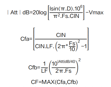
Component Selection Guidelines (for BUCK Converters)
- CD: 2–4 × CIN
- ESRD: √(LF / CIN); use high‑ESR capacitors or add series resistor
- LF: 1–47 μH (larger is better within current & size limits)
- CF: ceramic capacitor (better than electrolytic); calculated from attenuation, frequency, and circuit parameters
3. PCB Routing Guidelines for EMI
3.1 Input Capacitor Placement
Use electrolytic + ceramic capacitors at the input.
- Electrolytic: provides transient current
- Ceramic: filters high‑frequency spikes
Place ceramic caps close to VIN and GND pins; avoid vias.
3.2 Shorten Discontinuous Current Loops
In BUCK circuits, input current is discontinuous. Long loops increase parasitic inductance, causing voltage spikes and EMI.
Routing rules:
- CIN close to VIN and diode anode
- SW pin close to diode cathode
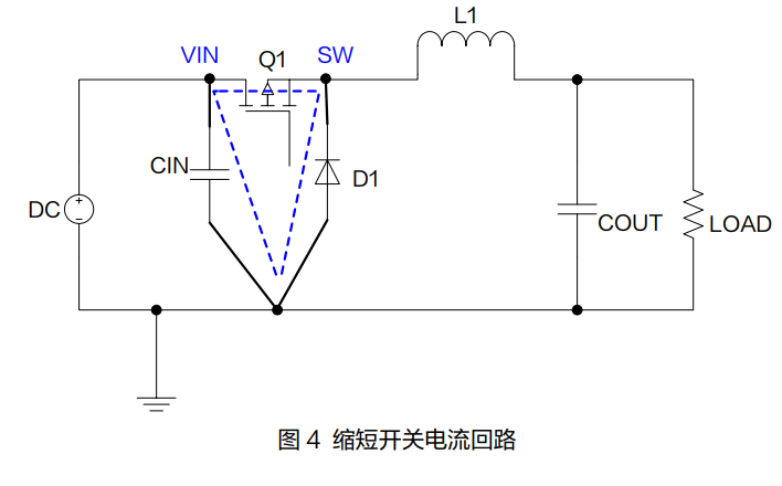
Figure 4 – Shortened switching current loop diagram
3.3 π‑Filter Routing Rules
- CF (ceramic cap) must be the only path for power & ground noise.
- Do NOT surround π‑filter components with large ground copper (creates parasitic capacitance Cx1, Cx2 that bypasses filtering).
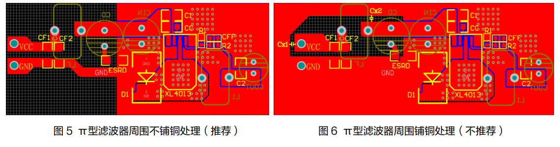
Figure 5 – Recommended: no ground copper around π‑filter
Figure 6 – Not recommended: ground copper around π‑filter (parasitic capacitance)