PCB process is critical in engineering, especially in large companies. It covers manufacturing constraints such as trace-to-via clearance, via aspect ratio, panel utilization, back-drilling depth, etc. This article summarizes the most commonly used PCB processes for designers.
PCB process is critical in engineering, especially in large companies. It covers manufacturing constraints such as trace-to-via clearance, via aspect ratio, panel utilization, back-drilling depth, etc. This article summarizes the most commonly used PCB processes for designers.
1. PCB Laminate Materials
The first consideration in PCB design is material selection. The most common is FR‑4, available in low‑/middle‑/high‑Tg grades (Tg = glass transition temperature). High‑Tg (≈170°C) is preferred for most designs.
Materials are classified by Dk (dielectric constant) and Df (dissipation factor). Lower Df means lower dielectric loss and higher cost.
Frequency & Loss Grade
- >20 GHz: Dk<3.0, Df<0.004
- 10–20 GHz: Dk 3.0–3.8, Df 0.004–0.008
- 5–10 GHz: Dk 3.8–4.1, Df 0.008–0.015
- **<5 GHz**: Dk>4.1, Df 0.015–0.020
- General purpose: Dk>4.1, Df≥0.020 (e.g., standard FR‑4)
Common materials:
- Standard: FR‑4 (TU662, IT158, etc.)
- Mid‑loss: Megtron4, TU872LK
- Low‑loss: Megtron6, TU883 (for >10 Gbps high‑speed signals)
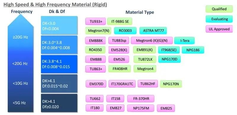
Figure 1 – PCB laminate material classification by frequency, Dk, and Df
2. Surface Finishes
Surface finish protects pads from oxidation and improves solderability.
- OSP: Organic solderability preservative (low cost, short shelf life)
- ENIG (Electroless Nickel Immersion Gold): Most widely used; excellent oxidation resistance, stable for >3 months storage
- Lead‑free process: Environmentally friendly, standard for most PCBs
3. Via‑in‑Pad (VIP)
A process that places vias
directly inside component pads to save routing space for high‑density fanout.
Cost increase: ~300–400 RMB per square meter.
Widely used in HDI and BGA designs.
4. Back‑Drilling
Used in high‑speed PCB design to
eliminate via stubs that cause signal reflection and insertion loss.
Extra stub copper is drilled out from the inner layer side.
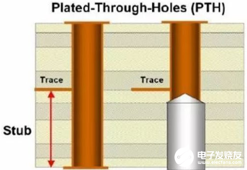
Figure 2 – Back‑drilling principle showing via stub removal
5. Solder Mask Defined (SMD) Opening / Copper Exposure
Used for power devices like MOSFETs to enhance heat dissipation.
Solder mask is removed from the backside to expose copper, allowing heat to transfer through vias to the other side of the PCB. A heat sink can be added for further cooling.
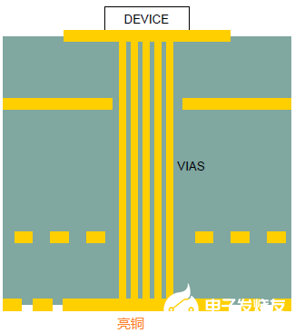
Figure 3 – Solder mask opening on MOSFET backside with exposed copper and thermal vias
About Maxipcb
Maxipcb empowers innovators to turn cutting-edge technologies into reality.
We offer one-stop solutions for design, simulation, testing, PCB manufacturing, component procurement and SMT assembly, enabling efficient development, rapid deployment and risk control across the full product lifecycle.Serving the world in communications, industrial automation, aerospace, automotive, semiconductor and beyond, we build a safer, more connected future together.


