A clear understanding of "makeup" of PCB: the essential difference between solder mask and solder mask.
A clear understanding of "makeup" of PCB: the essential difference between solder mask and solder mask.
When designing PCB in Altium Designer(AD), we often see Solder Mask and Paste Mask in the stack manager. What exactly are they? Why do they always appear in pairs? Simply put, they can be understood as "two different clothes" worn to complete different tasks in the process of PCB production and assembly.
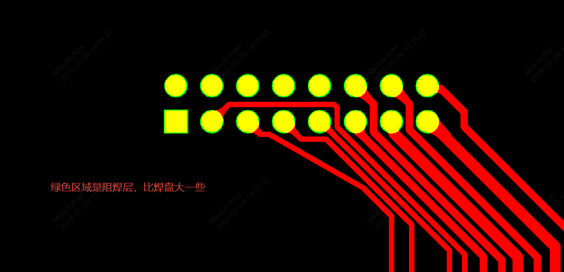
The core conclusion comes first:Solder Mask: Also called green oil layer, it is the non-wiring layer of the circuit board. Used to make silk screen stencil, where no welding is needed, it is coated with solder resist. Because of the fluidity of solder at high temperature when soldering a circuit board, a layer of solder resist must be coated where it is not needed to be soldered to prevent the solder from flowing and overflowing and causing short circuit.
Paste Mask: It is a non-wiring layer, which is used to make steel mesh, and the holes in the steel mesh correspond to the solder joints of SMD devices on the circuit board. When surface mount (SMD) devices are soldered, the steel mesh is first covered on the circuit board (corresponding to the actual pads), then the solder paste is coated, and the excess solder paste is scraped off with a scraper to remove the steel mesh, so that the solder paste is added to the pads of SMD devices, then the SMD devices are attached to the solder paste (manually or by a mounter), and finally the SMD devices are soldered by reflow oven.
Let's start a detailed analysis below.
First, solder mask: the "insulation protective clothing" of PCB.1. What is it?Solder resist, commonly known as "green oil", is a thin, high-temperature resistant polymer coating covering the surface of copper foil conductor on PCB. In AD, we define it through two layers: Top Solder Mask and Bottom Solder Mask.
2. Core function: prevent welding (short circuit prevention, oxidation resistance)Insulation protection: Covers almost all copper foil areas except pads, vias, etc., to prevent short circuit caused by accidental bridging of adjacent wires by solder during welding.
Anti-oxidation corrosion: protect copper wire from air and moisture corrosion and oxidation in long-term use.
Improve reliability: reduce the risk of circuit failure in harsh environment.
3. Design logic in AD: "Negative film output"This is the key to understand the solder mask. What you "paint" on the solder mask layer means "there is no window here, so you should paint it with green oil"? No! On the contrary.
Objects (lines, fills) in AD: stand for "windowed area". That is, solder resist ink is not applied here, and the copper skin (usually pad) below is allowed to be exposed for welding.
Default: By default, all areas on the PCB are covered with solder mask.
Your operation: If you need a pad or area to be soldered, you must place an opening in the same shape (usually slightly larger) on the solder mask. AD usually automatically generates solder mask openings for pads.
Simple memory: "something" on the solder mask = "window opening" here = "no green oil" here = "weldable" here.
Second, the welding aid layer: the "solder paste mold" of SMT chip.1. What is it?Welding aid layer, more accurately called "solder paste layer" or "steel mesh layer" It is not the actual coating on PCB itself, but the drawing used to make the Stencil needed for solder paste printing, the key process in SMT (surface mount technology) production line. In AD, it is defined by Top Paste Mask and Bottom Paste Mask.
2. Core function: help welding (precise and quantitative application of solder paste)Define the position of solder paste: tell SMT production line: "Please print solder paste on the pad of PCB through steel screen only at the position of the opening of the welding aid layer."
Control the amount of solder paste: the size of the opening directly determines the amount of solder paste, which is very important for the welding quality (especially for precision chips such as BGA and QFN).
3. Design logic in AD: "Positive output"This logic is much more intuitive than solder mask.
Objects (lines, padding) in AD directly represent "the opening shape of steel mesh", that is, the area where solder paste is to be printed.
Default: By default, all areas on the PCB are "no steel mesh openings".
Your operation: You need the SMD pad to be soldered, and AD will automatically create an opening with the same shape and usually the same size on the soldering aid layer. For pads that need more solder paste (such as heat dissipation pads), you can manually enlarge the opening of the flux layer.
Simple memory: "something" on the flux layer = "opening" on the steel mesh = "to print solder paste" here.
III. Comparison Table of Key Differences| Characteristic | Solder Mask | Paste Mask. |
| Physical form | Green insulating ink on PCB board | Stainless steel hollow template (steel mesh) for printing solder paste |
| Action link | Manufacturing process of PCB board (completed in board factory) | PCBA assembly (completed in SMT factory) |
| Core purpose | "Soldering resistance": insulation, protection and oxidation prevention. | "Welding aid": accurate positioning and quantitative application of solder |
| AD design logic | Negative logic: the graphics on the painting indicate that the green oil cannot be opened (window opening) | Positive logic: the graphics on the painting indicate that solder paste (opening) is to be printed. |
| Relationship with pad | The opening is usually 0.05-0.15mm larger than the single side of the pad to ensure that the edge of the pad is exposed and oil does not spill. | The opening is usually the same as or slightly smaller than the pad size to accurately control the amount of solder paste. |
| Main affected objects | All pads to be soldered (THT vias and SMD patches) | SMD surface mount pads only (solder paste is not required for through-hole components) |
| Visibility | After being made, it permanently exists on PCB and can be seen by naked eyes. | After printing the solder paste, the steel mesh is removed, only the solder paste remains on the pad, and disappears after reflow soldering. |
Imagine PCB assembly is like making a decorated cake:
PCB bare board: like a cake embryo.
Solder mask: like a layer of cream on a cake embryo. But you have to dig out the cream (solder mask and window opening) in advance where you need to put the fruit (solder components), so that the fruit can directly contact the cake embryo (copper plate) and stick.
Welding aid layer: it is like a hollowed-out paper pattern. You cover it on the cake, and squeeze jam (solder paste) through the opening of the paper mold only at the specific position (pad) where the cream is dug.
Final assembly: Then put the fruit (electronic components) in the position where there is jam, heat it as a whole (reflow soldering), the jam will solidify, and the fruit will be firmly adhered to the cake.
V. Key points of design inspectionBe sure to check the solder mask: make sure that there are no missing windows (which makes it impossible to weld) or windows are wrongly connected (which may lead to short circuit of welding).
Special device handling: For pads with large heat dissipation and requiring extra tin, remember to manually enlarge the opening of the flux layer.
Three-in-one: a standard SMD pad should be perfectly aligned by three layers in AD:
Top (or bottom) copper layer: defines the copper shape of electrical connection.
Top Solder: An opening slightly larger than the copper pad.
Top Paste: an opening the same as or slightly smaller than the copper pad.
Understanding and using solder mask and solder mask correctly is a key step to complete a PCB design with manufacturability, assembly and high reliability. I hope this article can help you completely distinguish the twins in the PCB world.
About MaxipcbMaxipcb inspires and empowers innovators and helps them bring world-changing technologies to life. We provide advanced design, simulation and testing solutions to help engineers complete development and deployment faster in the whole product life cycle, while controlling risks. Our customers are all over the world, such as communication, industrial automation, aerospace and national defense, automobile, semiconductor and general electronics. We join hands with customers to accelerate innovation and create a safe and interconnected world. 
