It is well known that reasonable laminated structure and continuous reference plane can effectively suppress EMI problems, but sometimes the design involves the problem of analog and digital signal isolation.
It is well known that reasonable laminated structure and continuous reference plane can effectively suppress EMI problems, but sometimes the design involves the problem of analog and digital signal isolation.
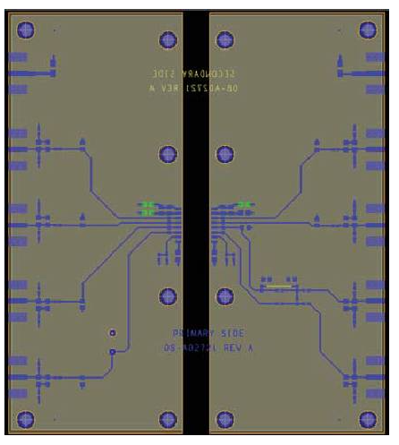
figure 1
Fig. 1 is a power conversion chip, in which one side is a digital signal and the other side is an analog signal. The separation of digital signals and analog signals helps to reduce the mutual interference between digital signals and analog signals. However, the middle separation area leads to the discontinuity of the reference plane, which leads to the problem of EMI.
Experienced designers may add Stitching Capacitance or magnetic beads between analog low and digital ground in this case. Usually, ceramic capacitors are used in these cases. However, adding capacitance will bring some unfavorable factors:
1. As the capacitor is a discrete device, the capacitor will add additional pad and via, and both pad and via will increase parasitic inductance.
2. Due to the small capacitance, the installed ceramic capacitor has a small effective space. Capacitors need to be installed in proper positions.
3. The frequency range in which the mounting capacitor works is generally lower than 200MHz.
The PCB is designed so that the power plane and the ground plane are tightly coupled as far as possible, and the coupling plane capacitance is formed between two adjacent planes. Can we have a way to separate the analog ground from the digital ground and make the noise on the separated plane better coupled to the ground plane? The method is shown in the following figure:
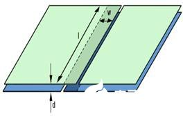
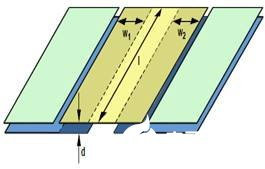
Figure 2 Figure 3
Fig. 2 and fig. 3 show two plane coupling modes.
The upper and lower planes form an overlapping area in the dividing area, and the overlapping area will form a coupling plate capacitor, which can not only separate the analog and digital areas, but also link the analog and digital areas together through the coupling plate capacitor.
The capacitor for by that plane has the following characteristic:
1. The parasitic inductance is small, and in addition, the capacitance is uniformly dispersed in the plane overlapping area.
2. The frequency range of planar coupling capacitor is wider.
3. Buried capacity plane has nothing to do with whether the plane is power plane or ground plane.
4. The buried structure is preferably located in the inner layer of the board. The surface layer or bottom layer will reduce the effect of plate coupling capacitance.
The two methods in Figure 2 and Figure 3 have their own advantages and disadvantages. The capacitance per unit plane in Figure 2 is large, but if the whole board is divided in this way, the PCB board is easy to break. This method is suitable for small area division. The capacitance per unit area in Figure 3 is small, but the PCB formed is firm. The space used for the board is large.
Fig. 4. Divided regions form planar coupling capacitors.
Remark: Calculation of planar coupling capacitance, taking Figure 4 as an example:
Figure 4 can be seen as the result of the series connection of the left and right two coupling capacitors in dark yellow.
C=(c1*c2)/(c1+c2), where c1 c2 is the left and right coupling capacitors respectively, assuming that the left and right coupling capacitors are equal, C1=c2=(ε*s)/d, where ε=ε_0*ε_r, ε_0 is the vacuum dielectric constant of 8.854*1e-12F/m, ε. S is the overlapping area, such as the dark yellow area in Figure 4, and D is the distance between overlapping areas.
Edadoc Company has a design that uses this scheme. In the design, the overlapping area is 4300mil long and 250mil wide, which is brought into the formula:
C=(4.5*(8.854*e-12)*4300*0.0254*(10e-3)*250*0.0254*(10e-3))/(5.12*0.0254*(10*e-3))=212pf
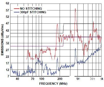
Fig. 5 forms a comparison chart of the measured data of 330pf stitched capacitor and no stitched capacitor.
About MaxipcbMaxipcb inspires and empowers innovators and helps them bring world-changing technologies to life. We provide advanced design, simulation and testing solutions to help engineers complete development and deployment faster in the whole product life cycle, while controlling risks. Our customers are all over the world, such as communication, industrial automation, aerospace and national defense, automobile, semiconductor and general electronics. We join hands with customers to accelerate innovation and create a safe and interconnected world. 


