The design shall meet the requirements of manufacturability, assemblability and maintainability, facilitate detection and rework during debugging, and enable easy disassembly of components
The design shall meet the requirements of manufacturability, assemblability and maintainability, facilitate detection and rework during debugging, and enable easy disassembly of components, following the guidelines below:
-
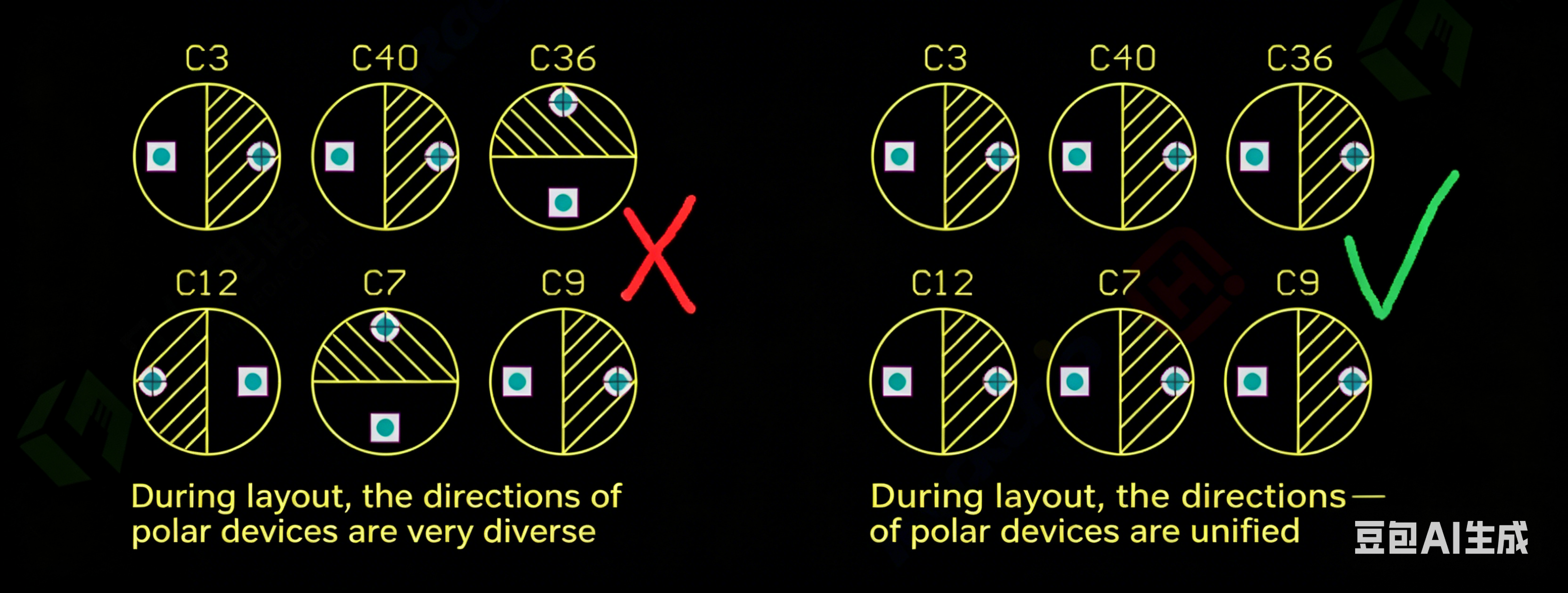
The orientation of polarized components should not exceed two types, and it is best to unify the orientation for all, as shown in [Illustration 1-1].
-
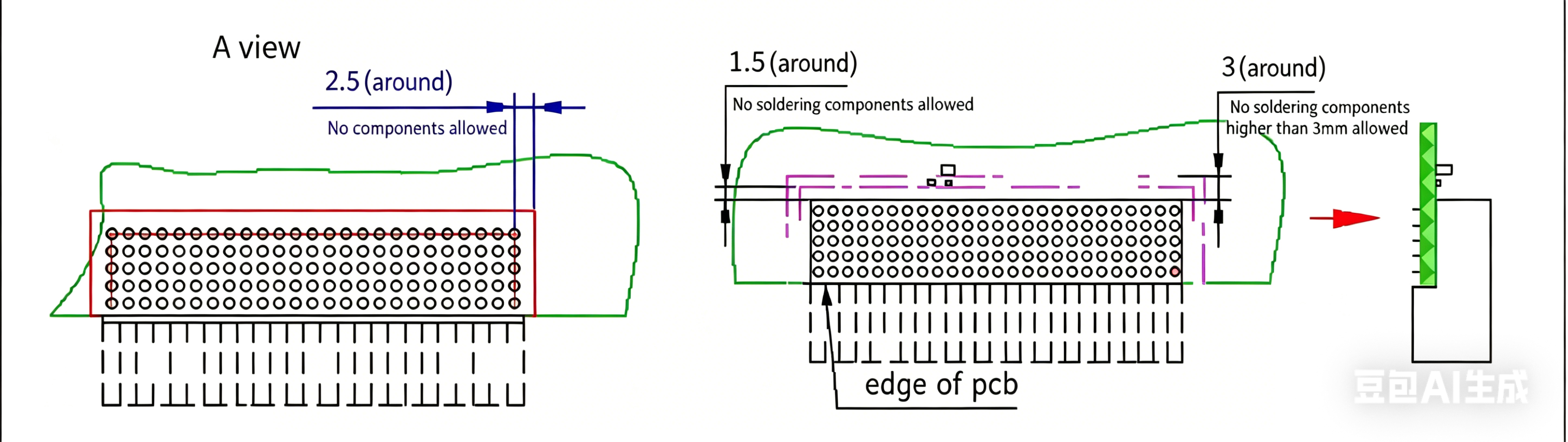
For male/female right-angle crimp connectors, the connector and crimp parts shall be on the same side. No tall components (over 3mm in height) shall be placed within 3mm around the crimp parts, no soldered components within 1.5mm around them, and no any components within 2.5mm of the crimp pins on the back of the crimp parts, as shown in [Illustration 1-2].
-
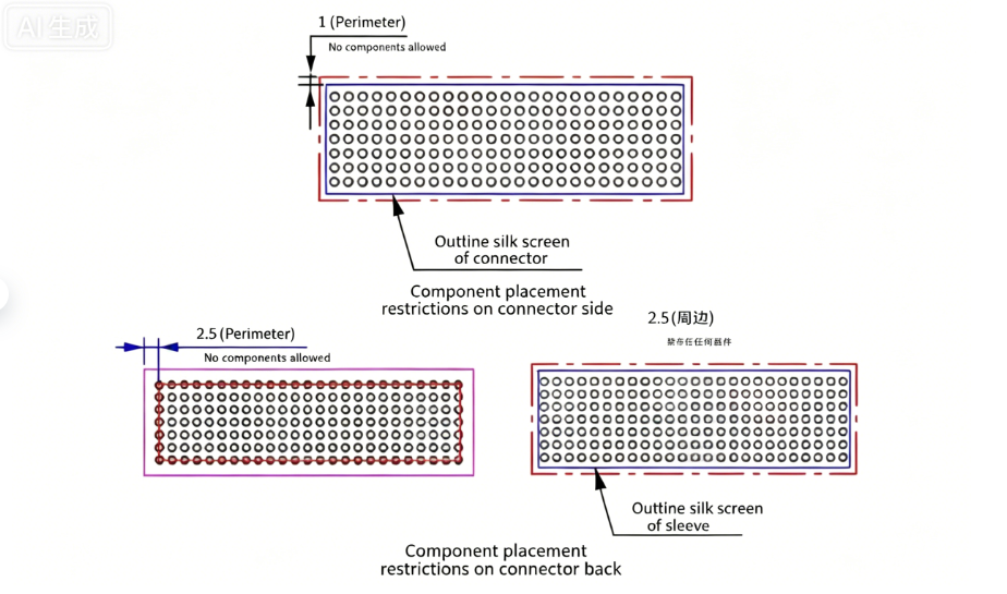
For male/female straight crimp connectors, no any components shall be placed within 1mm around the crimp parts. If a sheath is to be installed on the back, no components within 1mm around the corresponding area; if no sheath is installed, no components within 2.5mm of the crimp pins, as shown in [Illustration 1-3].
-
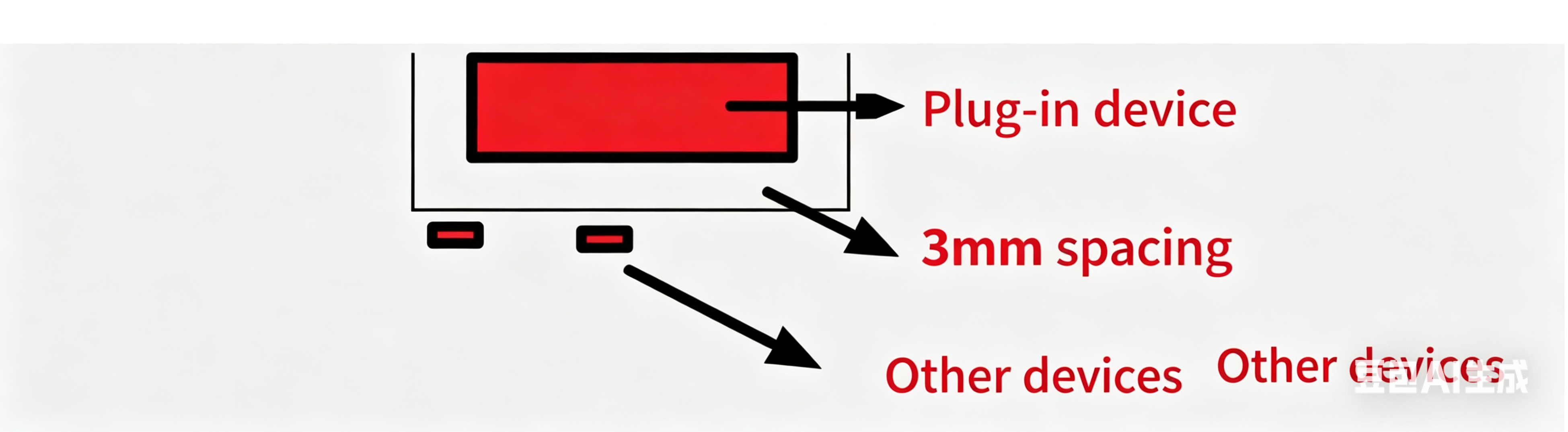
For conventional post-soldered components (connectors), a spacing of at least 1.5mm shall be maintained between the component and the connector when placed on the same layer, and a spacing of at least 3mm when placed on the back layer. Try not to place SMD components within 3mm of pluggable devices or board edge connectors to prevent component damage caused by stress during connector plugging and unplugging, as shown in [Illustration 1-4].
-
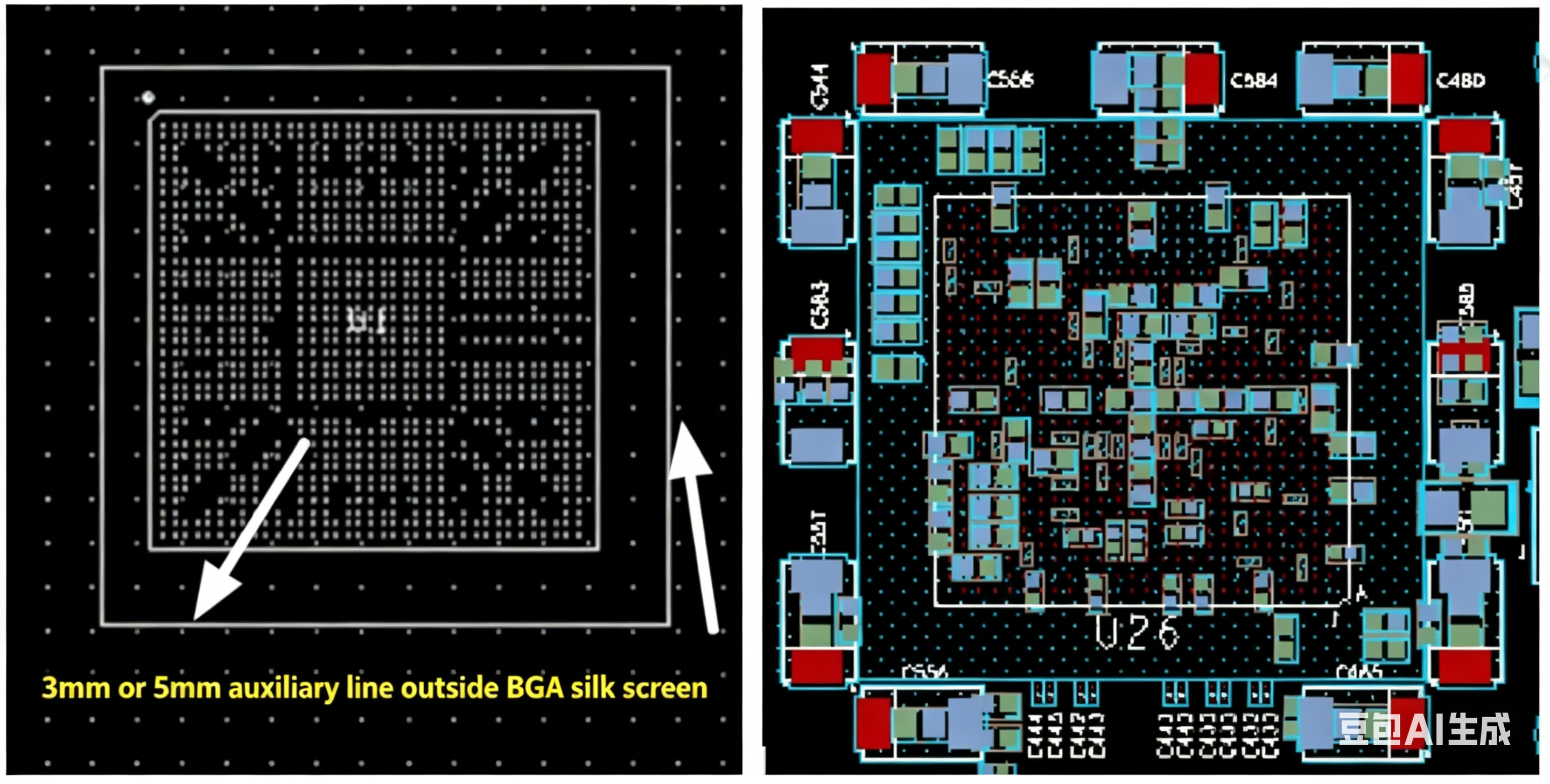
For BGA components: components on the same side shall be placed more than 5mm from the BGA component. In case of space constraints, the spacing can be reduced to more than 3mm, as shown in [Illustration 1-5].
-
Power filter capacitors for BGA components shall be placed on the back layer, as close as possible to the corresponding power pins, and at the symmetrical center of two adjacent pads of the BGA (some customers require that the BGA pads should not be covered to avoid missing detection during X-ray inspection), as shown in [Illustration 1-6].
-
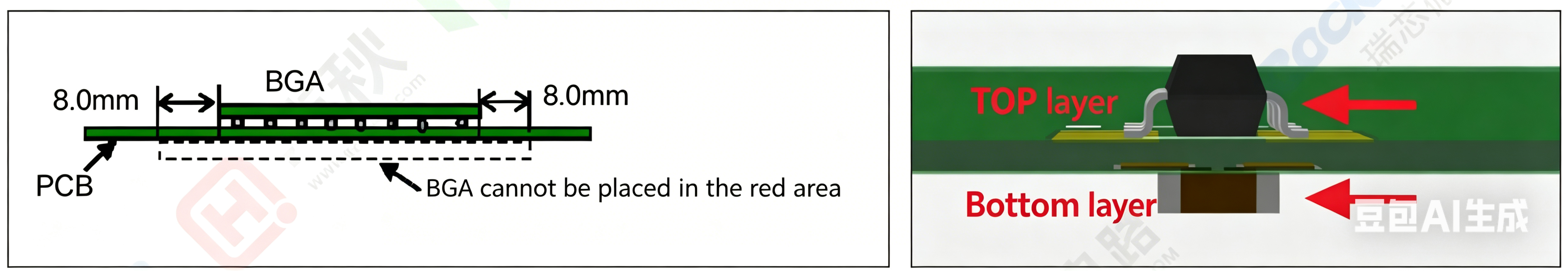
For double-sided placement with BGA components: generally, BGA components are not allowed to be placed on the back layer. If BGA components have to be placed on the back layer, no BGA components shall be placed within the 8mm projection range around the front BGA component, as shown in [Illustration 1-7].
-
For double-sided component placement: unless specially required, large components and chips shall be uniformly placed on the TOP layer, and passive components (resistors and capacitors) with sizes 0805, 0603 and 0402 on the bottom layer, as shown in [Illustration 1-8].
-
Small components (resistors, capacitors and Chip-type components) shall not be surrounded by tall components, and sufficient space (at least 3mm on both sides) shall be reserved for easy disassembly, as shown in [Illustration 1-9] and [Illustration 1-10]. For the layout principle of tall and short components, tall components shall be placed behind short ones and arranged along the direction of minimum wind resistance to prevent air duct blockage.
Schematic of Component Layout Requirements
Layout of Chip-type Components Surrounded by Tall Components
-
For metal-housed components, metal parts of different properties (such as heat sinks and shielding covers) or metal-housed components shall not touch each other or other components, and a minimum spacing of 1mm shall be ensured to meet the installation space requirements, as shown in [Illustration 1-11].
-
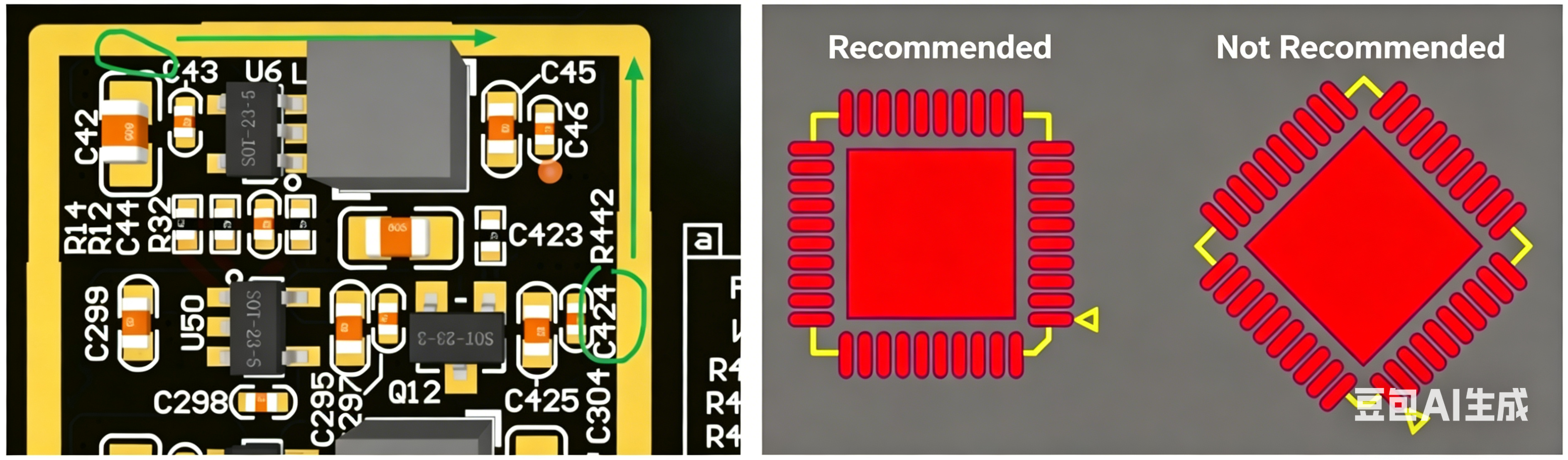
The recommended orientation for component placement is 0° or 90°; do not place components at a 45° angle unless special circumstances require it, as shown in [Illustration 1-12].
1mm Spacing Between Components and Shielding Covers
Component Placement Angles (Recommended & Not Recommended)
-
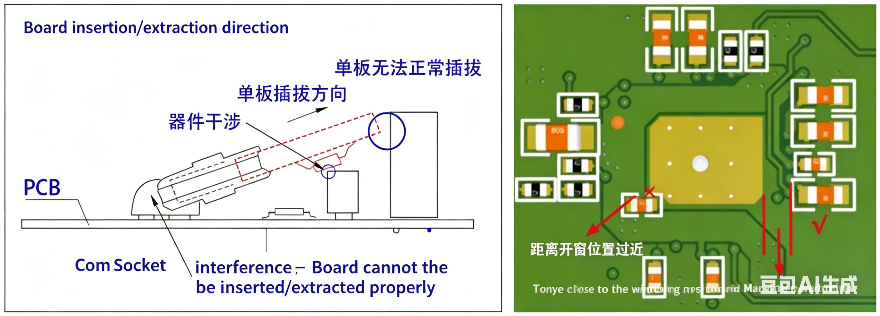
Operable space shall be reserved between components (e.g., for obliquely inserted memory modules) to facilitate plugging and unplugging operations, as shown in [Illustration 1-13].
-
For PCBs with windowing requirements: components shall be placed at least 2mm away from the windowed areas during layout, as shown in [Illustration 1-14].
Reserved Operable Space Between Components
Layout Spacing Requirement Between Components and Windowed Areas
-
A 5mm conveyor edge is not required if there are no SMD components within 5mm of the board edge, so as to save board material. If there are SMD components in this area, it is recommended to add a process auxiliary edge for the customer. Generally, the long edge is used as the conveyor edge; if the ratio of the short edge to the long edge is more than 80%, the short edge can also be used as the conveyor edge. If component layout cannot meet the conveyor edge width requirement (no placement within 5mm of the board edge), an auxiliary edge shall be added. The general width requirements for auxiliary edges: 5mm for non-panelized PCBs, and a minimum of 8mm for panelized PCBs. If the breakaway tab panelization method is adopted, attention shall be paid to the parameter setting of the breakaway tabs.
-
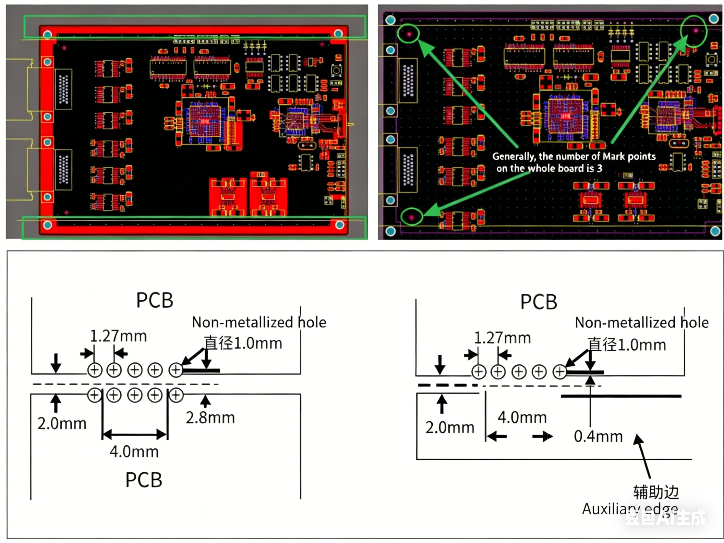
Before delivery, it is mandatory to check the layout of Mark points, including sufficient quantity and a spacing of more than 5mm from the board edge, as shown in [Illustration 1-15].
 About Maxipcb
Maxipcb empowers innovators to turn cutting-edge technologies into reality.
We offer one-stop solutions for design, simulation, testing, PCB manufacturing, component procurement and SMT assembly, enabling efficient development, rapid deployment and risk control across the full product lifecycle.Serving the world in communications, industrial automation, aerospace, automotive, semiconductor and beyond, we build a safer, more connected future together.


