Point 1: Distant feedback differential wiring of power supply voltage with large current.Voltage detection is divided into feedback detection and feedback detection. Generally, the small current power supply adopts near-end feedback, and the following circuit is the detection circuit. The voltage divider resistor and feedback line are placed near the output (output capacitor) of the power supply, and the single-ended signal feedback is enough.
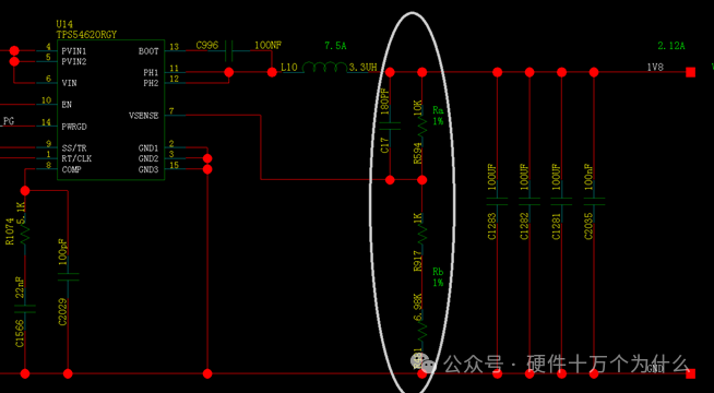
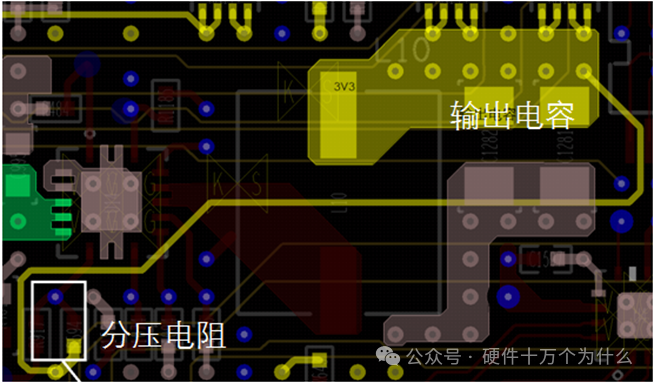
Generally, the high current power supply adopts near-end feedback, and the following circuit is the detection circuit. (If there is a voltage divider, the voltage divider is placed close to the controller) The main function of this pair of differential lines is to suppress common-mode interference, so there is no requirement for the line length difference of the differential pair.
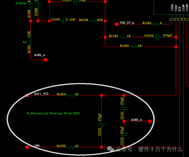
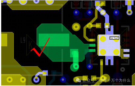
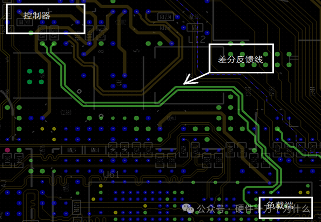 Point 2: Power supply current sampling differential wiring
The power supply current is sampled as a weak signal, which requires differential wiring and is far away from interference sources. Wrong wiring demonstration:
0.9V is mainly used to provide core power for two FPGA on a single board. The current is estimated to be 17.1A, and the current is relatively large. Therefore, it is doubtful whether the voltage of 0.9V drops due to overcurrent, so the 0.9V current is tested. The test results show that the current is indeed overcurrent (the actual test is less than 12A), but it does not reach the overcurrent point (25A) set in the schematic diagram.
The correct way: from both ends of the inductor to the middle lead, walk into a differential line, and place the conversion circuit as close as possible to the controller.
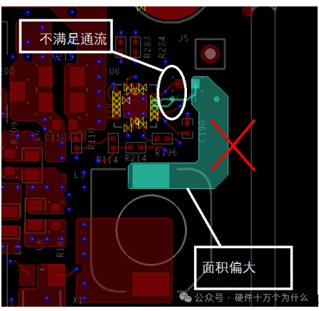
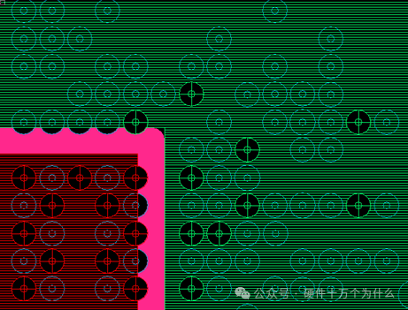
 Point 3: The area of 3:SW plane (Phase plane) should be as small as possible on the premise of ensuring the flow passage.
The Phase plane, that is, the connection network between the D pole of the lower tube and the S pole of the lower tube, constantly jumps between 0V and 12V, which has great external radiation and large current. According to the output current, the flow passage is calculated to ensure the flow passage, and at the same time, the area is small under the premise of meeting the flow passage.
The wrong wiring diagram is as follows:
Interference with other pins and networks, the minimum EN is only 1.14V, which leads to power failure by mistake.
After outgoing line, reduce the area of Phase plane as much as possible while ensuring the flow capacity, and stay away from easily disturbed signals. As shown in the figure below.
 Point 4: Power output current capacity needs to be checked.
Focus on checking vias and line widths: There are tools to calculate the relationship between throughflow and line widths, and the interconnection technology of throughflow capacity of vias has been experimented. The result of the experiment is that a 10MIL via can pass 2.7A current. In the design process, considering the factors such as voltage drop and reliability of power supply, we usually design a via as 1-1.5A..
At the same time, we need to pay attention to whether the positive and negative copper sheets are interrupted (BGA, dense vias, and whether there is a high-speed bus at dense vias). The original complete power plane will be hit by dense vias, which will not meet the flow requirements.
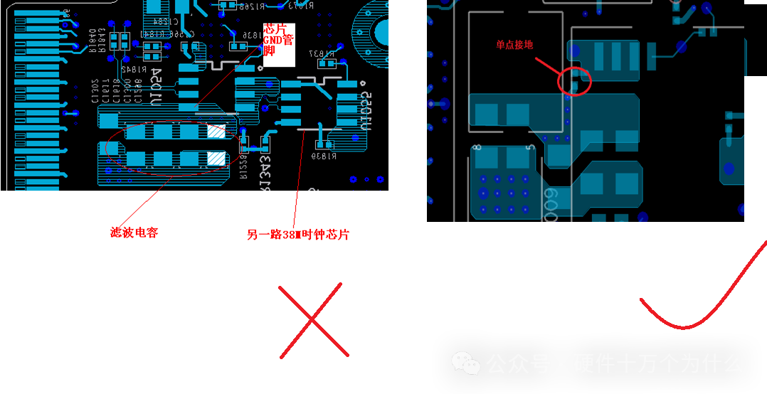
 Point 5: The GND of the chip cannot be grounded with the GND of the power supply filter capacitor (especially the filter capacitor that needs to be far away from the input power supply).
It is found that there is interference on the GND pin of the chip, and then it is confirmed that the interference of the power filter capacitor affects the differential input of the chip through the GND pin in common ground.
After testing the differential input terminal of the 38.88M clock line transceiver, it was found that the input differential signal was interfered. Later, when looking at the PCB, it was found that the GND pin of the chip was grounded with the filter capacitors of four 12V power supplies on the bottom surface, so it was found that there was interference on the GND pin of the chip. When the GND pin of the chip was pried up and connected to the ground of another nearby capacitor, the interference was obviously reduced. It is preliminarily determined that the noise on the power supply filter capacitor passes through the common ground plane, and the noise is directly connected in series from the chip GND pin, thus causing the input differential signal of the chip to be disturbed. Due to the interference of the chip's GND, the level of GND is directly raised, resulting in the interference of the differential input, and no abnormality has been found in the single-ended output for the time being. See figure for PCB routing.
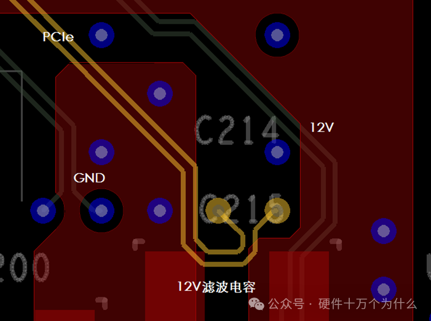
 Point 6: High-speed signals and sensitive signals are far away from input power supply and input GND.
The 12V PCIe 11 lane is too close to the 12V power supply plane, which is coupled to noise, causing it to drop to 1X or os to drop the disk.
The error demonstration is as follows:
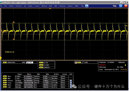
 Point 7: Inductive isolation is recommended for DCDC input with high current.
The eye diagram is very poor, and my eyes are not open at all.
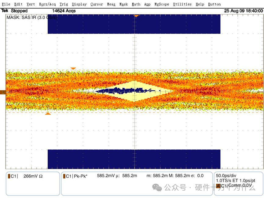
Root cause analysis:
Switching noise on 12V is coupled to the 1V1 plane. The switching noise of MOS transistor of VID power supply affects the input 12V of the previous stage. The reference ground of 1.1V is 12V, and the interference on 12V is coupled to the 1.1V plane.
Solution:
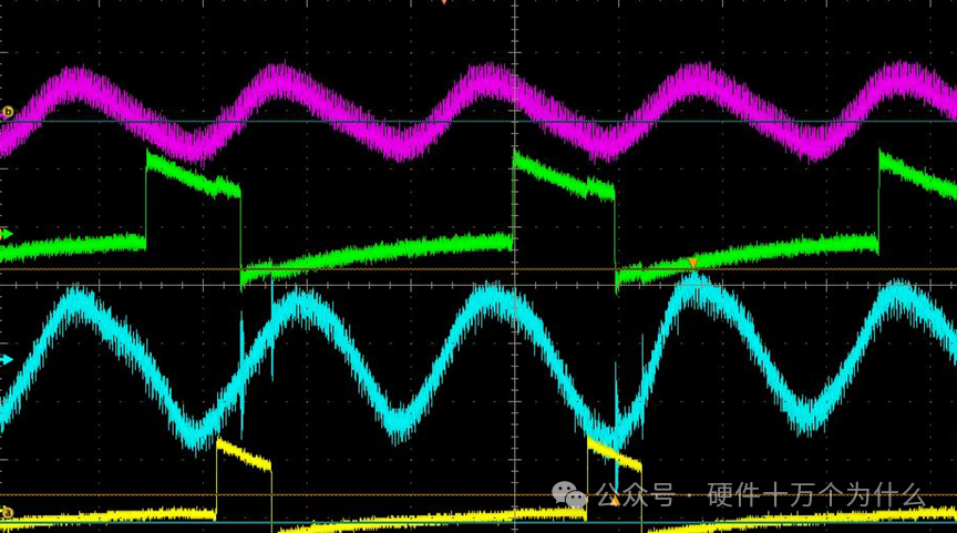
L-type filtering is adopted. A 1uH inductor is connected in series with the 12V input of VID, and a 470u capacitor is connected. The noise of measuring VID on 1.1V plane is completely filtered out. The phenomenon is also eliminated. Point 8: Place the input capacitor near the upper MOSFET.
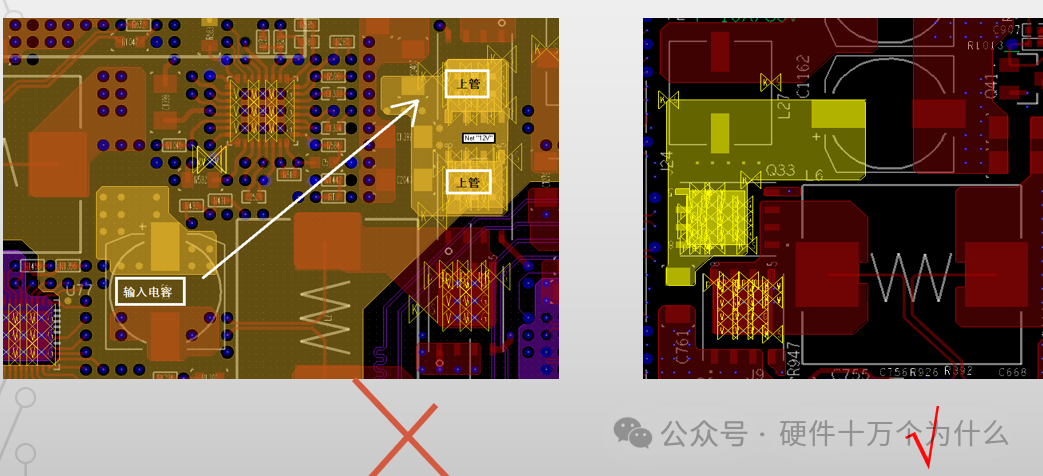
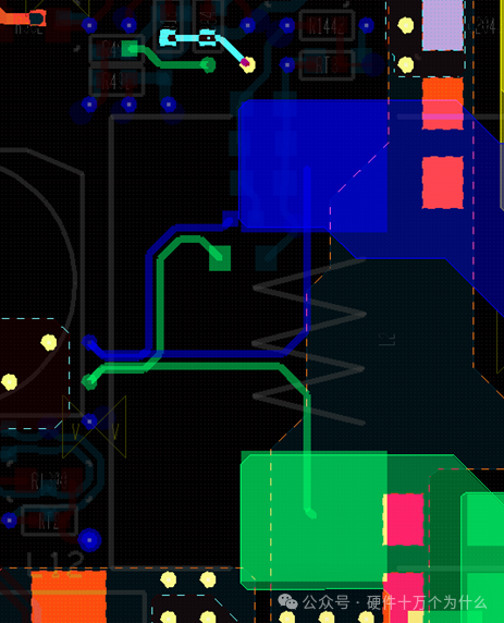
In the process of switching power supply, the red current loop is shown in the figure below when the upper tube is opened; The time when the lower tube is open is the purple current loop in the figure below. However, the two periods are superimposed together, and the part passing through the upper tube and the lower tube is a current loop with large current jump, while the current jump amplitude passing through the inductor is not large (blue waveform).
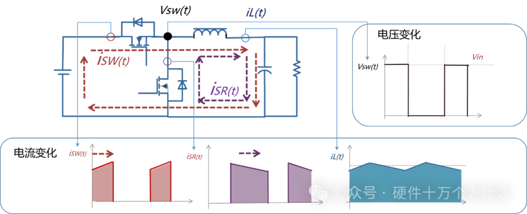
So we regard the loop of upper tube and lower tube and input capacitor as an interference loop.
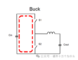
Therefore, we should place the input capacitor near the upper tube and the lower tube to minimize the area of this ring.
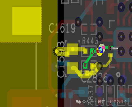
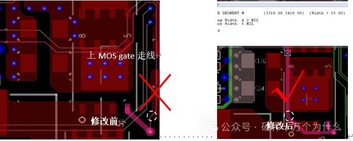
Point 9: the gate and boot capacitor traces should be as short and thick as possible.The gate drive of mos transistor has large switching voltage difference and large instantaneous current, so short and thick lines should be taken as far as possible when wiring, so as to reduce the interference along the lines and the inductance effect of the lines, and ensure the reliable opening and closing of MOS transistor, generally 15mil or more. If there is not enough space, the interconnection will also take the size of 10mil.
The pink highlighted line in the picture on the left below is the driving trace of the upper MOS tube. The wiring width of this trace in the inner layer is only 4.2mil, and the line length is not the shortest. The number of MOS transistors of switching power supply used on the board is not large, so it is necessary to check the wiring of driving lines one by one, especially whether the wiring width still meets the width requirements after layer change.
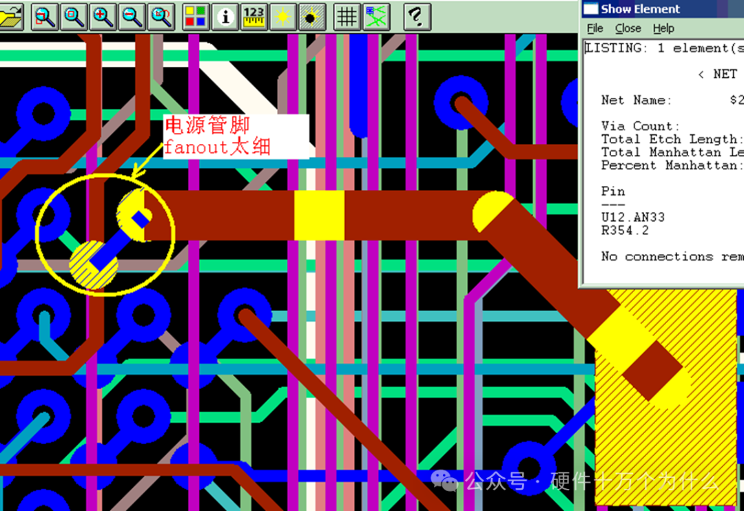
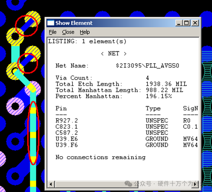
 Point 10: The line widths of diodes, inductors, magnetic beads and RC filtered resistors should be consistent;
As shown in the figure below, after the magnetic beads are isolated, power is supplied to the four power pins of the device, and the wiring is too thin, with a width of only 5 mil;

In the figure below, the core power cord meets the requirements, but fanout is too thin;
As shown in the figure below, after the PLL is filtered by magnetic beads, the wiring is too long and too thin, and fanout is too thin;
 About Maxipcb
Maxipcb empowers innovators to turn cutting-edge technologies into reality.
We offer one-stop solutions for design, simulation, testing, PCB manufacturing, component procurement and SMT assembly, enabling efficient development, rapid deployment and risk control across the full product lifecycle.Serving the world in communications, industrial automation, aerospace, automotive, semiconductor and beyond, we build a safer, more connected future together.


