For electronic equipment, it will generate a certain amount of heat when working, so that the internal temperature of the equipment will rise rapidly. If this heat is not dissipated in time, the equipment will continue to heat up, the device will fail due to overheating, and the reliability of electronic equipment will decline. Therefore, it is very important to heat the circuit board well.
For electronic equipment, it will generate a certain amount of heat when working, so that the internal temperature of the equipment will rise rapidly. If this heat is not dissipated in time, the equipment will continue to heat up, the device will fail due to overheating, and the reliability of electronic equipment will decline. Therefore, it is very important to heat the circuit board well.
 1. Add heat dissipation copper foil and copper foil with large area power supply.
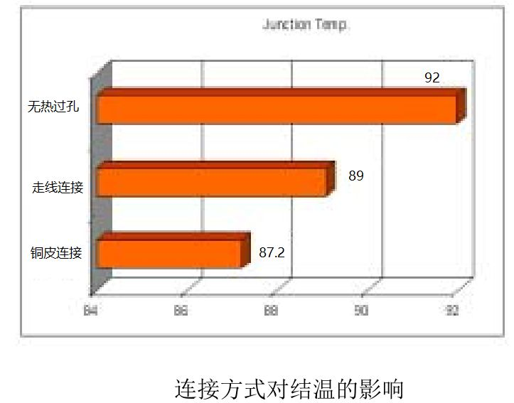
According to the above figure, it can be seen that the larger the area of connecting copper skin, the lower the junction temperature.
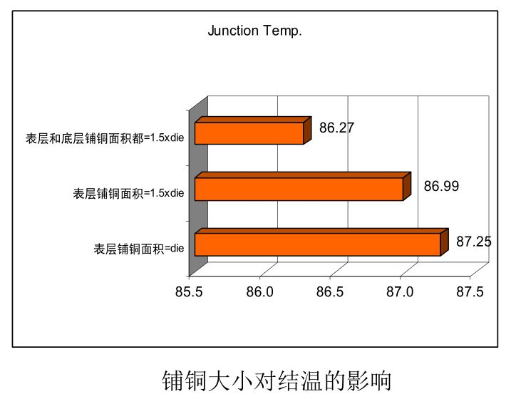
According to the above figure, it can be seen that the larger the copper-clad area, the lower the junction temperature.
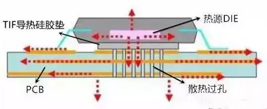
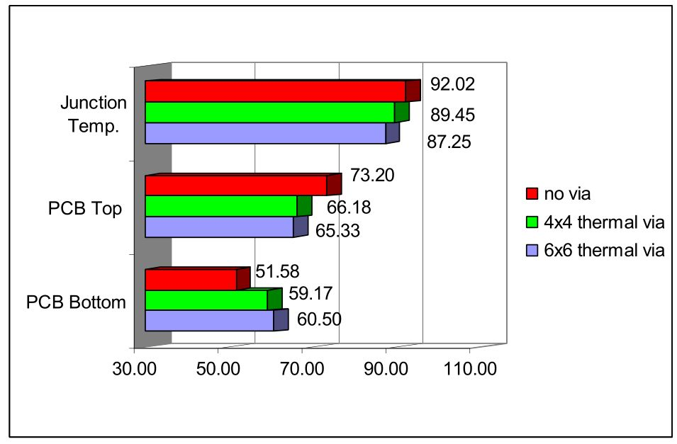
2. Hot viasThermal vias can effectively reduce the junction temperature of devices and improve the uniformity of temperature in the thickness direction of single board, which provides the possibility for adopting other heat dissipation methods on the back of PCB. Through simulation, it is found that the thermal power consumption of the device is 2.5W, the spacing is 1mm, and the design of 6x6 thermal vias in the center can reduce the junction temperature by about 4.8°C, while the temperature difference between the top surface and the bottom surface of PCB is reduced from 21°C to 5 C.. After the thermal via array is changed to 4x4, the junction temperature of the device increases by 2.2°C compared with 6x6, which is worthy of attention.
 3. Copper is exposed on the back of IC to reduce the thermal resistance between copper skin and air.
 4. PCB layout
Requirements for high-power and heat-sensitive devices.
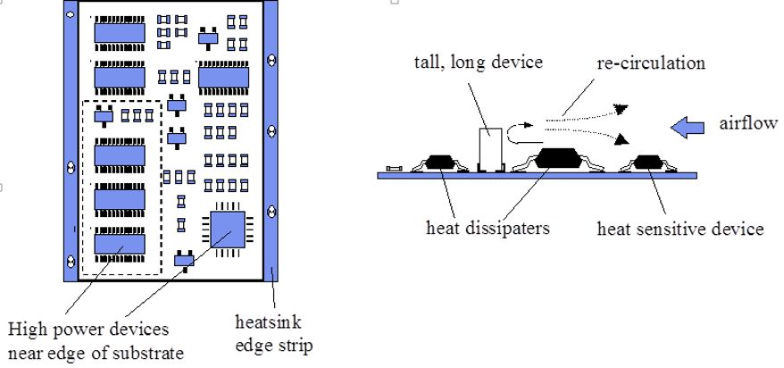
A, heat sensitive devices are placed in cold air area.
B, the temperature detection device is placed in the hottest position.
C devices on the same printed board should be arranged as far as possible according to their calorific value and heat dissipation. Devices with low calorific value or poor heat resistance (such as small signal transistors, small-scale integrated circuits, electrolytic capacitors, etc.) should be placed at the upstream (entrance) of cooling air flow, and devices with high calorific value or good heat resistance (such as power transistors and large-scale integrated circuits, etc.) should be placed at the downstream of cooling air flow.
D, in the horizontal direction, the high-power devices are arranged as close as possible to the edge of the printed board, so as to shorten the heat transfer path; In the vertical direction, the high-power devices should be arranged as close as possible above the printed circuit board, so as to reduce the influence of these devices on the temperature of other devices when they work.
E. The heat dissipation of the printed circuit board in the equipment mainly depends on air flow, so the air flow path should be studied in the design, and the devices or printed circuit boards should be configured reasonably. When air flows, it always tends to flow in a place with low resistance, so when configuring devices on the printed circuit board, it is necessary to avoid leaving a large airspace in a certain area. The configuration of multiple printed circuit boards in the whole machine should also pay attention to the same problem.
F, the device sensitive to temperature is best placed in the lowest temperature area (such as the bottom of the equipment), never put it directly above the heating device, and multiple devices are best staggered on the horizontal plane.
G, the device with the highest power consumption and the largest heat generation is arranged near the optimal heat dissipation position. Do not place devices with high heat on the corners and peripheral edges of the printed board unless a heat sink is arranged near it. When designing the power resistor, choose as large a device as possible, and make it have enough heat dissipation space when adjusting the layout of the printed board.
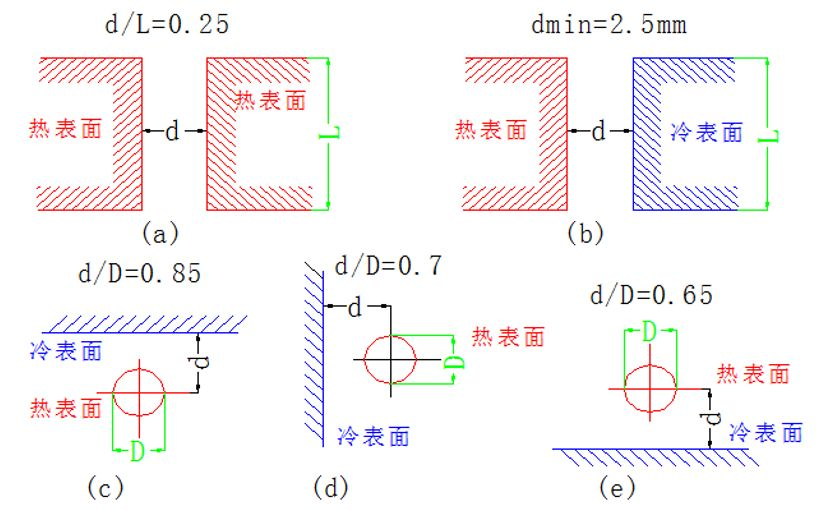
H. Suggestions on component spacing:
About Maxipcb
Maxipcb empowers innovators to turn cutting-edge technologies into reality.
We offer one-stop solutions for design, simulation, testing, PCB manufacturing, component procurement and SMT assembly, enabling efficient development, rapid deployment and risk control across the full product lifecycle.Serving the world in communications, industrial automation, aerospace, automotive, semiconductor and beyond, we build a safer, more connected future together. 


