It's almost half a year since I arrived in the new energy automobile industry, and I've had a little experience of "one after another". Where there is a market, there will be competition, and as an important part of it, the existence form of power semiconductor devices has been discussed a lot (relative to this industry).
Talk about the presentIt's almost half a year since I arrived in the new energy automobile industry, and I've had a little experience of "one after another". Where there is a market, there will be competition, and as an important part of it, the existence form of power semiconductor devices has been discussed a lot (relative to this industry). In the end, what kind of packaging, performance specifications, price and so on, it seems that there are only a few mainstream forms:
Single pipe, HPD, plastic-sealed half bridge (such as DCM) and TPAK are relatively common; Like double-pulse water-cooled DSC, eMPack, Viper, etc., they belong to niche markets. Among them, HPD is the most widely used module packaging form, and the others are not poor in performance, but can not be used. At the moment of "volume", cost seems to be in the primary position.
There is no strict dividing line between rolling up and rolling down. Under the same circumstances, I squeeze more limits in performance, which is also a kind of rolling up; Under the same conditions, my performance is far ahead, but the price is high, which seems to be better. Everyone is very concerned about the development cycle and the cost of trial and error, so it has been improved on the basis of the original maturity.
But in the big environment, the current practice is understandable, but those who can not forget innovation are still admirable. In any case, the future is changeable, and we will personally experience its changes.
PCB embedded power moduleThe PCB embedded power module shown by Wei Pai Technology at the ATC New Energy Power Forum mentioned at the beginning is a way to innovate on the basis of traditional module packaging. Several years ago, some papers have discussed the related packaging forms, including Infineon, which has also been shown before.
Embedding technologyIn fact, PCB embedding is basically the same as our common module packaging form, which can be considered as a technology with higher integration and higher power density. Just like the multi-layer PCB, the power semiconductor chip is embedded in the multi-layer PCB, and at the same time, the drive and control circuits can be arranged in other layers to get a highly integrated solution.
Embedded brief process:The connection of chips is similar to that of common semiconductors. The chips are soldered or sintered to the substrate, which can be copper foil, high-current PCB, or a substrate with isolation effect like a ceramic substrate. The simple schematic diagram is as follows,
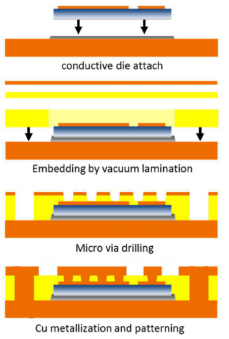
Embedding itself is accomplished by vacuum lamination of FR4 prepreg (glass fiber with B-grade epoxy resin) layers. The structured prepreg layer is used to compensate the height of the mold connection and the mold, and the whole layer provides the required isolation for the electrical layer above the mold. In addition, the copper foil needed in the metallization process is also applied. Embedding itself is carried out by lamination in a standard multilayer laminator.
Laser drilling is used to create the contact with the embedded mold, which needs careful control and parameterization to avoid damaging the chip. Blind passing through thick copper substrate or thick copper layer is usually by mechanical drilling. Subsequently, the microchannel is filled in the copper plating process, and then the structure of the electric layer is formed by photolithography and etching copper.
The appearance of the printed circuit board with embedded components is the same as that of the traditional circuit board. Therefore, in the subsequent process, we can not only deal with the additional signal layer, but also apply the solder mask and surface finish to install more components on the embedded module, and we can also add additional heat sinks or different types of embedded modules to the module.
Integrated drive and control circuit
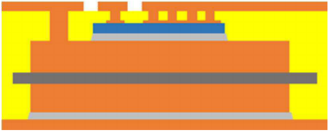
The embedded power module can be connected with the control board by sintering lamination technology (SLT) to form a PCB with more layers, as shown in the following schematic diagram.
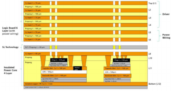
Logic PCB is composed of six layers, each layer has through holes, micro-through holes and 70µm thick copper. At the bottom, the area connected between the logic and power PCB by sintering lamination technology (SLT) is partially plated with silver.
The idea of SLT is to produce electrical (or thermal) contact at the same time, and to fill the cavity between the contact points with the resin of prepreg (PCB starting material) in one process step. In this process, silver sintering paste is applied to the respective connections, usually by template or screen printing. In order to fill the cavity, it is necessary to make a prepreg layer with an opening at the position where silver is to be sintered. The whole stack of sinter paste and prepreg added with sil is placed on each other. The joining process is carried out in a multi-layer laminating press. In the first stage, silver is sintered and flows, thus filling the cavity. In the second stage, the epoxy resin of prepreg is completely thermally crosslinked. After this lamination process, the connection of various layers is completed.
summarizeIt can be seen that the embedded PCB packaging technology not only reduces the volume, but also reduces the long line connection between the traditional module and the control board, and at the same time reduces the parasitic parameters of the loop, which is of great benefit to the switching speed and switching loss of silicon carbide.
But the development of everything needs a process and an opportunity to produce, and maybe we can see it in the car before long. Just like chatting with a friend, he asked me what packaging I could do, such as empack, Viper or PCB embedded, etc. I said what I had done and there was no market. He said, "Those are the future."
About Maxipcb
Maxipcb empowers innovators to turn cutting-edge technologies into reality.
We offer one-stop solutions for design, simulation, testing, PCB manufacturing, component procurement and SMT assembly, enabling efficient development, rapid deployment and risk control across the full product lifecycle.Serving the world in communications, industrial automation, aerospace, automotive, semiconductor and beyond, we build a safer, more connected future together.


