In the design of high-speed PCB boards, via design is a crucial factor. A via consists of a hole, a pad area around the hole, and an isolation area on the power layer, and is generally classified into three types: blind vias, buried vias, and through-holes. By analyzing the parasitic capacitance and parasitic inductance of vias during PCB board design, this article summarizes key precautions for via design in high-speed PCB boards.
Currently, the design of high-speed PCB boards is widely applied in fields such as communication, computers, and image processing. The design of all electronic products with high technological added value pursues characteristics like low power consumption, low electromagnetic radiation, high reliability, miniaturization, and light weight. To achieve these goals, via design becomes a critical element in high-speed PCB board design.
1. Vias
Vias are an essential component in the design of multi-layer PCB boards. A via is mainly composed of three parts: a hole, a pad area surrounding the hole, and an isolation area on the power layer. The manufacturing process of a via involves depositing a layer of metal on the cylindrical wall of the hole through chemical plating, which connects the copper foils that need to be interconnected on each inner layer. The top and bottom surfaces of the via are formed into ordinary pad shapes, which can be directly connected to the circuits on the top and bottom layers or left unconnected. Vias can serve the functions of electrical connection, component fixation, or positioning.
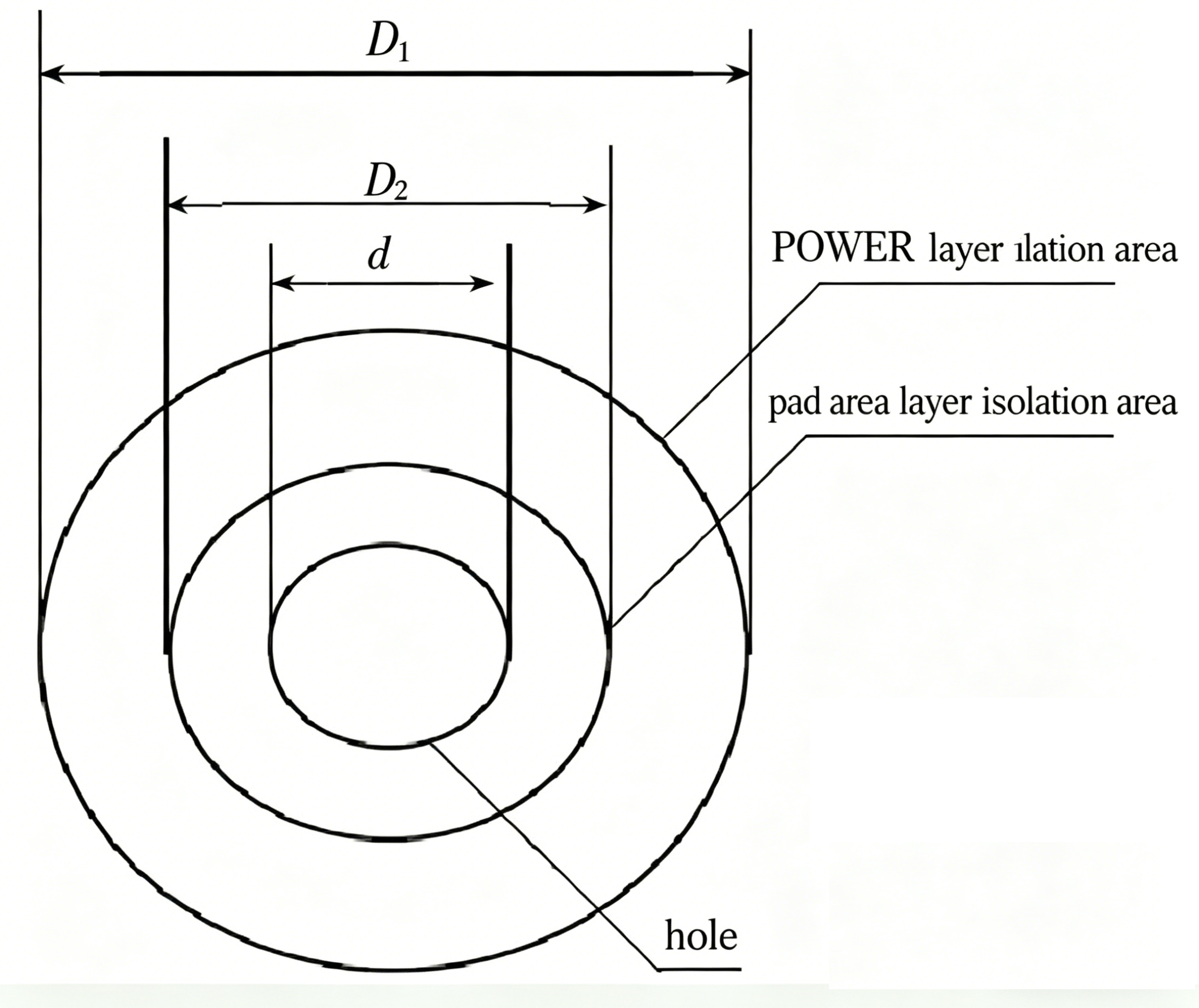
(Power Layer Isolation Area, Pad Area Around the Hole, Hole)
Vias are generally divided into three categories: blind vias, buried vias, and through-holes.
- Blind vias: Located on the top and bottom surfaces of a printed circuit board with a certain depth, used to connect surface circuits to the underlying inner-layer circuits. The depth and aperture of the blind via usually do not exceed a specific ratio.
- Buried vias: Connection holes located in the inner layers of a printed circuit board that do not extend to the board's surface.
Both blind and buried vias are located in the inner layers of the circuit board and are fabricated using through-hole forming technology before lamination; multiple inner layers may even be stacked during the via formation process.
- Through-holes: Holes that penetrate the entire circuit board, used for internal interconnection or as mounting and positioning holes for components. Through-holes are widely used in general printed circuit boards due to their easier manufacturing process and lower cost.
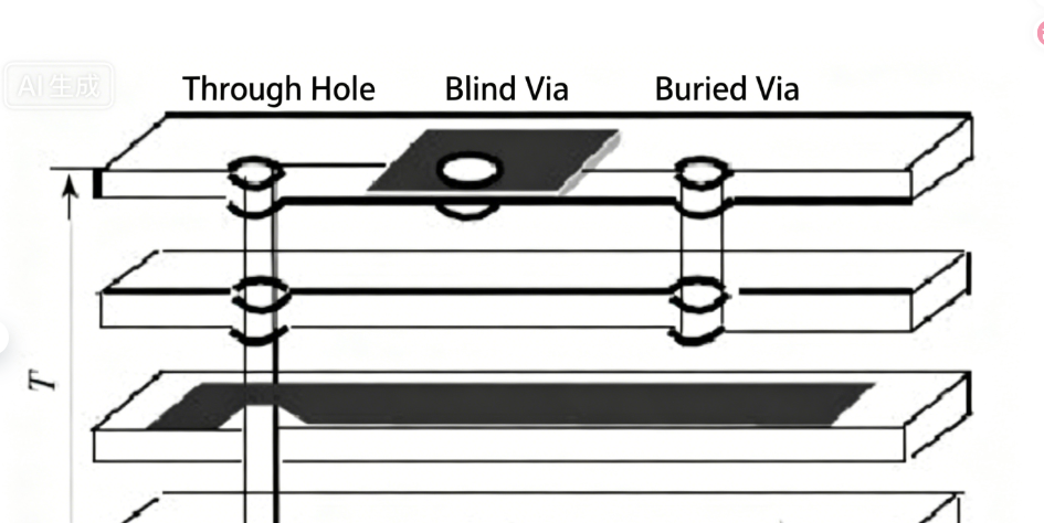
(Through-hole, Blind via, Buried via)
2. Parasitic Capacitance of Vias
Vias inherently have parasitic capacitance to the ground. If the diameter of the isolation hole of a via on the ground plane is D2, the diameter of the via pad is D1, the thickness of the PCB is T, and the dielectric constant of the board substrate is E, the parasitic capacitance of the via is approximately calculated by the formula:
C=1.41ETD1/(D2-D1)The main impact of the parasitic capacitance of vias on the circuit is extending the signal rise time and reducing the circuit speed; the smaller the capacitance value, the smaller the impact.
3. Parasitic Inductance of Vias
Vias also have inherent parasitic inductance. In the design of high-speed digital circuits, the harm caused by the parasitic inductance of vias is often greater than that of parasitic capacitance. The parasitic series inductance of vias will weaken the effect of bypass capacitors and reduce the filtering efficiency of the entire power supply system. If L refers to the inductance of the via, h is the length of the via, and d is the diameter of the central drill hole, the parasitic inductance of the via is approximately calculated by the formula:
L=5.08h[ln(4h/d)+1]It can be seen from the formula that the diameter of the via has a minor impact on the inductance, while the length of the via is the most significant factor affecting the inductance.
4. Non-Penetrating Via Technology
Non-penetrating vias include blind vias and buried vias. The application of blind and buried vias in non-penetrating via technology can greatly reduce the size and weight of PCBs, decrease the number of layers, improve electromagnetic compatibility, enhance the features of electronic products, reduce costs, and also make the design work more simple and efficient.
In traditional PCB design and processing, through-holes bring many problems. Firstly, they occupy a large amount of effective space; secondly, a dense cluster of through-holes creates huge obstacles for routing on the inner layers of multi-layer PCBs, as they take up the space required for wiring. Their dense penetration through the surface of power and ground layers also damages the impedance characteristics of the power and ground layers, rendering them ineffective. In addition, conventional mechanical drilling requires 20 times the workload compared to non-penetrating via technology.
In PCB design, although the sizes of pads and vias have been gradually reduced, if the board layer thickness is not reduced proportionally, the aspect ratio of through-holes will increase, which reduces reliability. With the maturity of advanced laser drilling technology and plasma dry etching technology, the application of small non-penetrating blind and buried vias has become possible. If the aperture of these non-penetrating vias is 0.3mm, the resulting parasitic parameters are about 1/10 of those of conventional vias, improving the reliability of PCBs. The use of non-penetrating via technology results in far fewer large vias on the PCB, thus providing more space for wiring.
The remaining space can be used for large-area shielding to improve EMI/RFI performance. At the same time, more remaining space can be used for partial shielding of components and key signal lines on the inner layers to achieve optimal electrical performance. The use of non-penetrating vias facilitates the fan-out of component pins, making it easy to route high-density pin components (such as BGA packaged components), shortening the connection length, and meeting the timing requirements of high-speed circuits.
5. Via Selection in Conventional PCBs
In conventional PCB design, the parasitic capacitance and inductance of vias have a minor impact on the design. For 1-4 layer PCB design, vias with specifications of 0.36mm/0.61mm/1.02mm (drill hole/pad/power isolation area) are generally preferred. For signal lines with special requirements (such as power lines, ground lines, clock lines, etc.), vias with specifications of 0.41mm/0.81mm/1.32mm can be selected, and vias of other sizes can also be used according to actual needs.
6. Via Design in High-Speed PCBs
From the above analysis of the parasitic characteristics of vias, it can be seen that in high-speed PCB design, seemingly simple vias can bring significant negative effects to the circuit design. To minimize the adverse effects caused by the parasitic effects of vias, the following measures can be taken in the design:
- Select reasonable via sizes. For multi-layer PCB design with general density, vias with specifications of 0.25mm/0.51mm/0.91mm (drill hole/pad/power isolation area) are preferred; for high-density PCBs, vias with specifications of 0.20mm/0.46mm/0.86mm or non-penetrating vias can be used; for power or ground vias, larger sizes can be considered to reduce impedance.
- The power isolation area should be as large as possible. Considering the via density on the PCB, the general standard is D1=D2+0.41mm.
- Signal traces on the PCB should avoid layer changes as much as possible, which means minimizing the number of vias.
- Using a thinner PCB helps reduce both parasitic parameters of vias.
- Vias should be placed as close as possible to the pins of power and ground; the leads between vias and pins should be as short as possible, as longer leads will increase inductance. At the same time, the leads for power and ground should be as thick as possible to reduce impedance.
- Place some grounded vias near the vias where signals change layers to provide a short loop for the signals.
Of course, specific problems need to be analyzed specifically in the design. Considering both cost and signal quality, designers always hope to use the smallest possible vias in high-speed PCB design, as this leaves more wiring space on the board. In addition, smaller vias have lower inherent parasitic capacitance, making them more suitable for high-speed circuits. In high-density PCB design, the use of non-penetrating vias and the reduction of via sizes both lead to increased costs, and the size of vias cannot be reduced indefinitely due to the limitations of PCB manufacturers' drilling, electroplating and other process technologies, which should be considered in a balanced manner in the via design of high-speed PCBs.

 (Power Layer Isolation Area, Pad Area Around the Hole, Hole)
 (Through-hole, Blind via, Buried via)