Taking 8-layer PCB as an example, this article briefly explains the definition of each layer and critical notes in practical PCB design.
Taking 8-layer PCB as an example, this article briefly explains the definition of each layer and critical notes in practical PCB design.
Two mainstream stacking structures for 8-layer PCB are introduced below:
Scheme 1
All signal layers refer to ground planes or power planes, delivering excellent EMI performance and stable controlled characteristic impedance for each signal layer.
- Signal 1: Component side, microstrip routing layer with premium routing performance
- Ground 1: Inner ground plane
- Signal 2: Stripline routing layer with optimal routing quality
- Power 1: Inner power plane
- Ground 2: Inner ground plane
- Signal 3: Stripline routing layer with optimal routing quality
- Power 2: Inner power plane
- Signal 4: Microstrip routing layer with premium routing performance
Scheme 2
The optimal stacking design for 8-layer PCB. Adopting multiple ground reference planes ensures superior noise absorption; however, only one single power plane is configured, limiting power distribution design for complex PCBs.
- Signal 1: Component side, microstrip routing layer with premium routing performance
- Ground 1: Inner ground plane
- Signal 2: Stripline routing layer with optimal routing quality
- Power: Inner power plane
- Ground 2: Inner ground plane
- Signal 3: Stripline routing layer with optimal routing quality
- Ground 3: Inner ground plane
- Signal 4: Microstrip routing layer with premium routing performance
Next, we build an 8-layer PCB in Altium Designer following Scheme 2. The stacking structure is shown in the figure below:
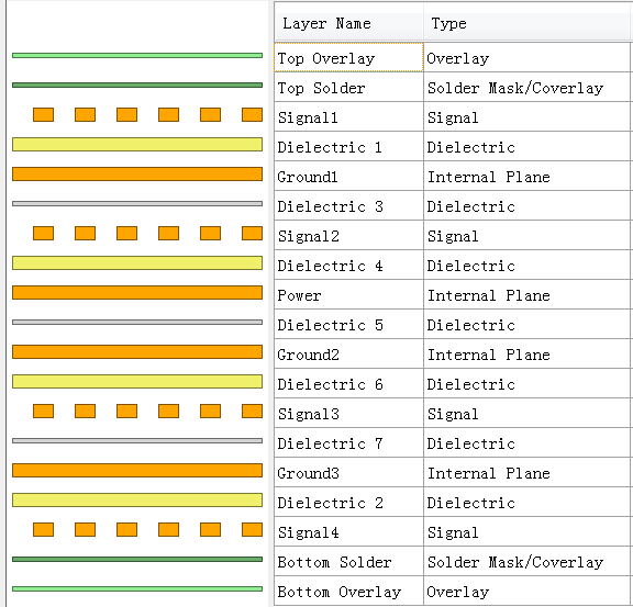
After configuration, Altium Designer generates the 8-layer PCB according to the above stacking rules. Apart from the 8 core layers, auxiliary layers are included: Mechanical 1, Top Paste, Bottom Paste, Drill Guide, Keep-Out Layer, Drill Drawing and Multi-Layer. The functions of each layer are specified as follows:
- Signal Layer: Core layer for electrical signal transmission.
- Ground Layer: Provides ground reference and return path for circuits.
- Power Layer: Supplies power to all electronic components on the PCB.
- Mechanical 1: Stores manufacturing & assembly information, including PCB outline, dimension markings, technical specifications, via data and assembly instructions.
- Top Overlay: Marks component outlines, designators, ratings, models and notes on the top side; visible after PCB fabrication.
- Bottom Overlay: Marks component outlines, designators, ratings, models and notes on the bottom side; visible after PCB fabrication.
- Top Paste: Used for stencil making for SMT soldering; only SMT pads on the top layer are displayed here (vias & through-hole pads excluded).
- Bottom Paste: Used for stencil making for bottom-side SMT soldering; only bottom SMT pads are displayed here (vias & through-hole pads excluded).
- Top Solder: Exposed copper areas (SMT pads, vias, through-hole pads) are defined here; other areas are covered with solder mask ink after production.
- Bottom Solder: Identical function to the top solder mask layer.
- Drill Guide: Defines drilling layouts and serves as critical reference for Gerber file generation.
- Keep-Out Layer: Sets electrical boundaries to restrict routing, via placement and component layout.
- Drill Drawing: Precisely marks drill hole coordinates for Gerber manufacturing.
- Multi-Layer: Displays cross-layer components such as through-hole pads and vias.
For design engineers, signal layers, power layers, ground layers, silkscreen layers and mechanical layers are the most commonly used. Auxiliary layers can be ignored in general design scenarios without special requirements.
About Maxipcb
Maxipcb empowers innovators to turn cutting-edge technologies into reality.
We offer one-stop solutions for design, simulation, testing, PCB manufacturing, component procurement and SMT assembly, enabling efficient development, rapid deployment and risk control across the full product lifecycle.Serving the world in communications, industrial automation, aerospace, automotive, semiconductor and beyond, we build a safer, more connected future together.

