The data sheets of most components contain recommended PCB packaging information and specify the aperture suitable for this component. This is the most practical method to select the aperture of PCB. However, some data sheets only provide the physical dimensions and pin diameter tolerances of components. In this case, how should we choose the aperture when we only create component packages based on these physical dimensions?
"The data sheets of most components contain recommended PCB packaging information and specify the aperture suitable for this component. This is the most practical method to select the aperture of PCB. However, some data sheets only provide the physical dimensions and pin diameter tolerances of components. In this case, how should we choose the aperture when we only create component packages based on these physical dimensions? "
 Introduction
In PCB design, the aperture and pad size of Through-Hole components are the key parameters that determine the final assembly quality and product reliability. Accurate aperture design is not only the basis of automatic assembly, but also the premise of ensuring excellent welding performance and long-term mechanical stability. Improper aperture selection may lead to a series of manufacturing problems, such as difficult component insertion, welding defects and potential reliability risks. This paper aims at systematically expounding the standard methods and core principles of PCB through-hole diameter design, so as to help engineers avoid risks in the design stage and improve the first-pass rate of products.
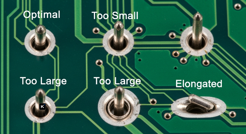
Basic principles of aperture designThe design of through-hole aperture must strike a balance between the physical size of component pins and the manufacturing process tolerance. If the aperture is too small, the components will not be inserted smoothly, which will increase the cost and risk of manual rework, and may even damage the component pins or PCB plates during forced assembly. On the other hand, if the aperture is too large, it will cause problems in the welding process, such as insufficient solder filling, component position deviation, and the decrease of mechanical strength of solder joints.
There is a simple application rule: add 0.2mm to the nominal pin diameter to get the appropriate aperture. Why 0.2mm? Why not only increase it by 0.05mm, or completely match the pin diameter? Because component manufacturers will apply tolerance ranges to physical dimensions. The actual size will be different from the nominal value.
The tolerance of most pin diameters is about 0.05 mm. The allowance of 0.2mm can reliably adapt to this change and ensure the stable insertion of components.
Of course, if we are more rigorous, we should follow the specifications of IPC 2221 (the latest version is IPC 2221B).
IPC2221: the industry standard for aperture design.The International Electronic Industry Association (IPC) provides authoritative guidelines for PCB design and manufacture. According to IPC-2221A/B and other related standards, the calculation of the hole diameter of the through hole is based on the following core formula:
Minimum Hole Size)= Max. Lead Diameter)+ Allowance.According to different application grades and component densities of products, IPC defines three levels of tolerance margins to meet different design requirements:
- Level A (universal design/first choice): provides the largest manufacturing tolerance, is suitable for most standard density product designs, and has the best manufacturability.
Calculation formula:
Maximum pin diameter+0.25mm (10 mils)
- Level B (Medium Density Design/Standard): It reduces the tolerance, is suitable for the design with high component density, and is a balanced choice between performance and manufacturability.
Calculation formula:
Maximum pin diameter+0.20mm (8 mils)
- Level C (High Density Design/Minimum): It provides minimum tolerance and is specially designed for high density or complex circuit boards with extremely limited space. The selection of this grade requires a higher technological capability of the manufacturer and needs careful evaluation.
Calculation formula:
Maximum pin diameter+0.15mm (6 mils)
Note: that when calculating, the Maximum pin size marked in the component Datasheet must be taken as the benchmark, not "Typical". This is a key preventive measure to avoid assembly problems caused by component batch differences.
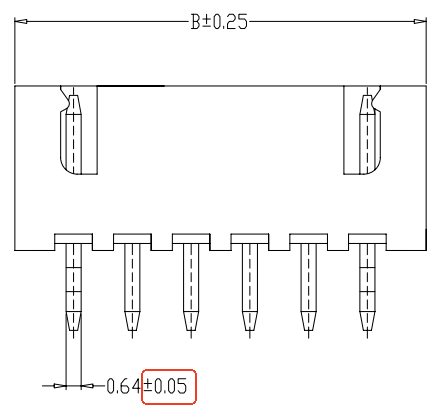
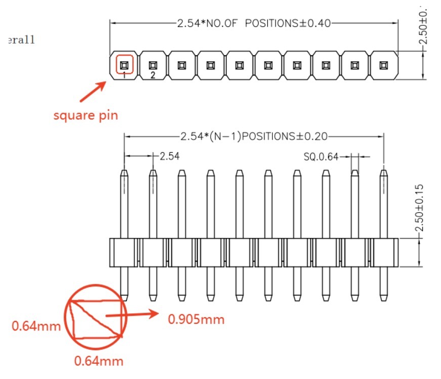
Processing method of non-circular pinFor a pin with a square or rectangular cross section, its effective diameter is its diagonal length. When designing, the maximum diagonal dimension should be determined by geometric calculation (Pythagorean theorem), and then it is substituted into the IPC formula as the "maximum diameter of the pin".
For a rectangular pin with cross-sectional dimensions a and b:
Maximum effective diameter (diagonal) = √ (a+b)
For example, if the aperture of PCB package is not recommended in the data sheet, the maximum effective diameter is √ (√(0.64²+0.64²) =0.905mm;; The reasonable package aperture value is 0.905 mm+0.2 mm = 1.1 mm.
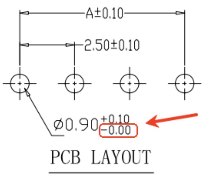
 Unilateral tolerance
If the data sheet only specifies a positive tolerance (for example, 0.9 mm+0.1 mm/0), use: Standard+All Positive Tolerances.
For example, the aperture in the figure below = 0.9 mm+0.1 mm = 1.0 mm.
 Collaborative design of pad size
After the aperture is determined, the matching Pad must be designed to ensure the formation of a reliable Annular Ring. The width of the annular ring directly affects the strength of the solder joint and the reliability of conduction. The calculation formula of pad diameter is usually:
Pad diameter = aperture +2× (minimum ring width requirement)+(manufacturing tolerance)
According to IPC standard, the minimum ring width should not be less than 0.15mm (6 mils). When designing, we should comprehensively consider the process capacity of the board factory and follow the principle of DFM to communicate with the manufacturers.
Improper design will cause potential manufacturing defects:
- Difficulties in assembly and pin damage: the small aperture directly leads to the failure of the automatic plug-in, and the manual correction process is easy to damage the pin or hole wall.
- Component position deviation: If the aperture is too large, the component may tilt or translate during transmission and Wave Soldering, which will affect the circuit performance and product appearance.
- Welding defects: Excessive Hole-to-Lead Ratio will hinder the normal filling of solder by capillary action, and it is easy to form holes, virtual welds or incomplete solder joints, which constitutes a long-term reliability hazard.
Concluding remarksAccurate PCB through-hole aperture design is a bridge between design and manufacturing. By following IPC standards and adopting rigorous design process, engineers can significantly improve the manufacturability, assembly efficiency and ultimate reliability of products, thus reducing production costs and speeding up the product listing cycle.
About Maxipcb
Maxipcb empowers innovators to turn cutting-edge technologies into reality.
We offer one-stop solutions for design, simulation, testing, PCB manufacturing, component procurement and SMT assembly, enabling efficient development, rapid deployment and risk control across the full product lifecycle.
Serving the world in communications, industrial automation, aerospace, automotive, semiconductor and beyond, we build a safer, more connected future together.


