In the field of PCB (printed circuit board) design, screen printing, as a key element on the surface of the circuit board, plays an important role. It provides engineers, production personnel and subsequent maintenance personnel with important information such as component number, location and installation direction, and is the core element to ensure the readability and convenience of the circuit board.
In the field of PCB (printed circuit board) design, screen printing, as a key element on the surface of the circuit board, plays an important role. It provides engineers, production personnel and subsequent maintenance personnel with important information such as component number, location and installation direction, and is the core element to ensure the readability and convenience of the circuit board.
A well-designed PCB screen printing mark can significantly improve work efficiency, reduce the risk of welding errors, and provide strong support for the production, testing and maintenance of circuit boards. However, in the actual design process, there are often some problems in screen printing polarity marks, which need our in-depth discussion and improvement.
one. Common problems of polarity mark in PCB screen printing
In the practice of providing DFA (Design for Assembly) audit services for many customers, we found that engineers have different habits of screen printing polarity marks. Some engineers use the intuitive "+/-"symbol to mark the positive and negative poles, while others use the triangle symbol of diode to indicate the direction of the positive and negative poles. However, there are still many signs with potential defects, which are easy to cause misunderstandings and bring troubles to the use and maintenance of circuit boards.
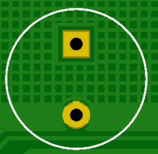
1..Mark polarity with dots.It is common to mark one side of the pad with a dot as a polarity symbol, but the problem is that different designers have different definitions of the polarity represented by the dot. For non-circuit board designers, this marking method is difficult to accurately judge the positive and negative poles, and it is easy to cause misunderstanding, which in turn affects the correct installation and maintenance of the circuit board.
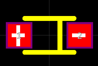
 2..Mark polarity with long and short silk screen lines on both sides.
Similar to dot marking, this marking method also makes it difficult for users to determine whether the pad on one side of the long line is positive or negative. In addition, in the actual drawing process, there may be only a slight difference in length between the silk screen lines on both sides, which undoubtedly further increases the difficulty for users to judge the polarity and weakens the proper function of silk screen marks.
 3. Missing silk screen mark
For plug-in components with polarity, some designers only change one of the via pads to a square pad to indicate polarity. However, it is different from the polarity requirement that the pin is represented by a square pad. These polarity pins do not clearly specify that the pin is the positive or negative electrode in the specification. Unless there is an obvious asymmetric contour on the screen printing of the device to assist the judgment, it is difficult to accurately judge the polarity direction for use, which brings great inconvenience to the welding or maintenance of the circuit board.
 TWO. Design suggestion of polarity mark for silk screen printing.
In order to effectively improve the identifiability and convenience of the circuit board, and enhance the intuition and accuracy of the polarity mark of screen printing, we suggest the following design methods.
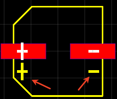
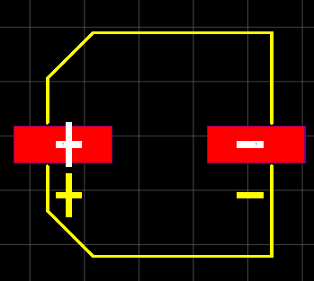
2.1 "+/-"marks polarity or "K" marks negative pole.The "+/-"symbol is a well-known expression of positive and negative poles, and it can be clearly marked on the circuit board, so that users can quickly and accurately identify the corresponding positions of positive and negative poles. This marking method is simple and clear, conforms to the public's cognitive habits, effectively avoids misunderstanding caused by fuzzy marking, and provides a strong guarantee for the installation, testing and maintenance of circuit boards.
 2.2 Mark polarity with a horizontal line on one side.
When the components are physically marked with horizontal lines of polarity, the polarity is correspondingly marked with horizontal lines on the PCB, so that users can intuitively judge the positive and negative poles. This design method echoes the physical characteristics of components, enhances the recognition and credibility of screen printing marks, and helps to improve the overall quality and reliability of circuit boards.
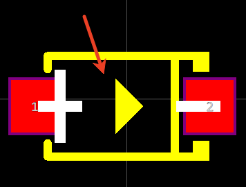
 2.3 Triangular symbol mark of secondary tube
The turn-on symbol of diode is an intuitive polarity representation method. By using the triangle symbol of diode to mark the polarity, the user can easily determine the positive and negative poles according to the conduction direction. This marking method not only conforms to the professional norms of electronic industry, but also provides clear and accurate guidance for engineers and production personnel to ensure the correct installation and welding of circuit boards.
 2.4 Draw silk-screen marks according to the physical outline.
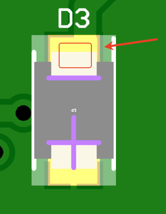
For the polarity plug-in which is not completely symmetrical, it is an effective auxiliary judgment method to add the screen-printed outer frame of its substance. In this way, users can accurately understand the installation direction of components according to the shape and direction of the screen printing frame, and then determine the polarity. This not only improves the efficiency of polarity judgment, but also enhances the standardization and professionalism of circuit board design.
To sum up, it is of great significance to simplify the PCB manufacturing and testing process and improve the overall quality of PCB by adopting a more intuitive and clear polarity design of screen printing marks. Therefore, we hope that the above skills can provide useful reference for your circuit board design.
About MaxipcbMaxipcb inspires and empowers innovators and helps them bring world-changing technologies to life. We provide advanced design, simulation and testing solutions to help engineers complete development and deployment faster in the whole product life cycle, while controlling risks. Our customers are all over the world, such as communication, industrial automation, aerospace and national defense, automobile, semiconductor and general electronics. We join hands with customers to accelerate innovation and create a safe and interconnected world. 


