For long‑distance high‑speed signals (especially backplanes), routing layer selection is critical to avoid excessive high‑frequency loss. This article compares microstrip (surface) and stripline (inner layer) routing using simulation.
For long‑distance high‑speed signals (especially backplanes), routing layer selection is critical to avoid excessive high‑frequency loss. This article compares microstrip (surface) and stripline (inner layer) routing using simulation.
1. Basic Concepts
- Microstrip: Signal routing on the outer layer (with solder mask above)
- Stripline: Signal routing between two ground planes (inner layer)
Their loss and performance differ due to dielectric and reference plane conditions.
2. Simulation Setup
Two stack‑up models were built for comparison:
Microstrip (Surface)
- Er1 = 4.2, H1 = 1.4 mil, TanD1 = 0.04 (solder mask)
- Er2 = 4.2, H2 = 4 mil, TanD2 = 0.022
- Trace width: 6.2 mil (for 50 Ω impedance)
- Length: 5000 mil
Stripline (Inner Layer)
- Er = 4.2, H = 20 mil, TanD = 0.022
- Trace width: 3.5 mil (for 50 Ω impedance)
- Length: 5000 mil
- Reference: GND on both sides
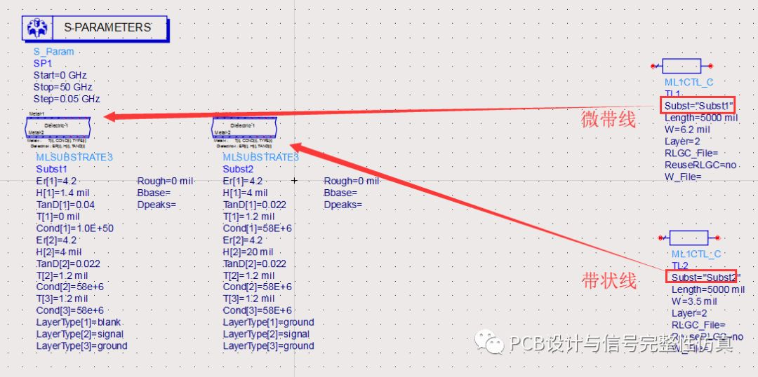
Microstrip and stripline stack‑up structure diagrams
Simulation conditions:
- Frequency range: 0–50 GHz
- Step: 0.05 GHz
- Port setup completed
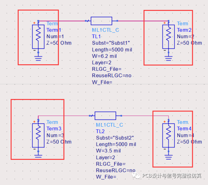
Simulation schematic with port connections
3. Simulation Results (FR‑4 Material)
Under standard FR‑4 (DF = 0.022):
- Microstrip (S21) shows lower loss than stripline (S43).
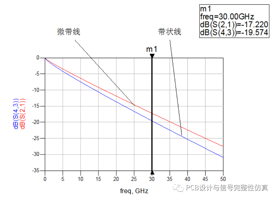
S‑parameter comparison plot (FR‑4 material)
4. High‑Speed Material Comparison
High‑speed materials have much lower DF (dissipation factor). DF was set as a variable and tuned from 0.022 down to 0.002.
At DF = 0.002 (high‑speed material):
- Stripline loss becomes lower than microstrip.
- The lower the DF, the larger the advantage of stripline over microstrip.
Reason: Solder mask (green oil) on the surface introduces significant extra loss for high‑speed materials.
Tuning tool interface and S‑parameter plot at DF = 0.002
5. Conclusion
- For standard FR‑4: Surface microstrip has lower loss.
- For high‑speed materials (low DF): Inner stripline is better for long‑distance high‑speed signals.
Practical design recommendation:
When using high‑speed laminates, route long‑haul high‑speed signals on
inner layers (stripline) to minimize transmission loss.
About Maxipcb
Maxipcb empowers innovators to turn cutting-edge technologies into reality.
We offer one-stop solutions for design, simulation, testing, PCB manufacturing, component procurement and SMT assembly, enabling efficient development, rapid deployment and risk control across the full product lifecycle.Serving the world in communications, industrial automation, aerospace, automotive, semiconductor and beyond, we build a safer, more connected future together.


