Flexible PCB materials need to support a variety of design and operational objectives: static or dynamic bending, compatibility with standard assembly processes, adaptability to simple manufacturing procedures, and achievement of high production yields. At first glance, flexible PCB materials may seem specialized, but a relatively small set of materials can be used for mass production of flexible and rigid-flex PCBs.
Flexible PCB materials need to support a variety of design and operational objectives: static or dynamic bending, compatibility with standard assembly processes, adaptability to simple manufacturing procedures, and achievement of high production yields. At first glance, flexible PCB materials may seem specialized, but a relatively small set of materials can be used for mass production of flexible and rigid-flex PCBs. In this guide, we will examine some basic characteristics of flexible PCB materials and how to use them to construct flexible/rigid-flex PCBs.
Substrates and Coverlays
The most common substrate used in rigid printed circuit boards is woven fiberglass impregnated with epoxy resin. It is essentially a fabric—though we refer to these boards as "rigid", individual laminated layers exhibit reasonable flexibility on their own. Cured epoxy resin imparts rigidity to the board, and such boards are generally referred to as organic rigid PCBs due to the epoxy resin used. This type of substrate lacks sufficient flexibility for many applications but may be suitable for simple components that do not require continuous movement.
Polyimide (PI) is the most common material of choice for flexible PCB substrates, offering excellent flexibility and extreme heat resistance.
Most flexible circuit applications require more flexible plastics than standard epoxy resins. Polyimide is the primary selection for two key reasons: it is highly flexible (cannot be torn or significantly stretched by hand, making it resistant to the rigors of product assembly processes) and boasts outstanding heat resistance. This makes it highly tolerant of multiple solder reflow cycles and relatively stable against expansion and contraction caused by temperature fluctuations.
Polyester (PET) is another commonly used flexible circuit material, yet it cannot withstand the high temperatures required for soldering. It is typically found in extremely low-cost electronic products where the flexible section features printed conductors (PET cannot endure the heat of lamination), and components are assembled without soldering—instead, electrical contact is established via pressure contact with isotropic conductive elastomers.
A notable example of PET's limitations is a timer radio product where the display never functioned properly due to poor connection quality of the flexible circuit. For this reason, we will focus on PI film for rigid-flex PCB applications (other materials are available but rarely used in practice).
PI and PET films, along with thin flexible epoxy and fiberglass cores, form the universal substrates for flexible circuits. The circuit then requires an additional film layer (typically PI or PET, sometimes flexible solder mask ink) as a coverlay. The coverlay insulates the outer surface conductors and prevents corrosion and damage, serving the same function as the solder mask on rigid PCBs.
PI and PET films range in thickness from 1/3 mil to 3 mil, with 1 mil or 2 mil being the standard. Fiberglass and epoxy substrates are significantly thicker, ranging from 2 mil to 4 mil.
Conductors
While the aforementioned low-cost electronic products may use printed conductors (usually a carbon film or silver-based ink), copper is the most typical conductor for flexible PCBs, with different forms of copper selected based on application requirements:
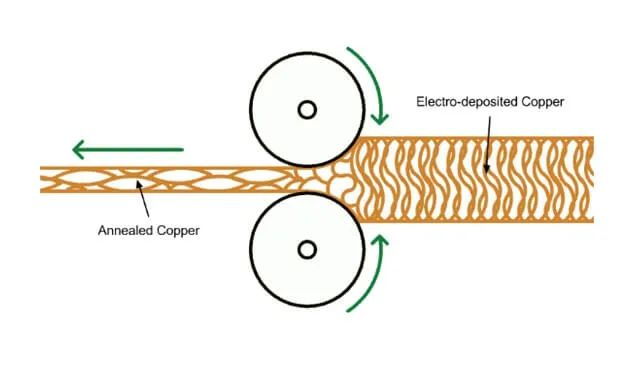
- Electrodeposited (ED) copper foil: This is the laminated copper foil commonly used for rigid PCBs, suitable for applications where the flexible section of the circuit is used only to eliminate cables and connectors (reducing manufacturing time and cost). It is also ideal for scenarios requiring heavier copper weights to keep high-current-carrying conductors at the minimum feasible width, such as planar inductors.
- Rolled Annealed (RA) copper foil: Copper is prone to work hardening and fatigue, so RA copper foil (a higher-grade option) is necessary for end applications involving repeated bending or movement of the flexible circuit. The additional annealing step significantly increases production costs, but annealed copper can withstand more stretching before fatigue cracking and exhibits greater elasticity in the Z-deflection direction—an essential property for flexible circuits that need to be continuously bent or rolled. This is because the rolling and annealing process elongates the grain structure in the planar direction.
Adhesives
Traditionally, adhesives are required to bond copper foil to PI (or other) films. Unlike typical FR-4 rigid PCBs, annealed copper has fewer surface "teeth", meaning heat and pressure alone are insufficient to form a reliable bond. Manufacturers supply pre-laminated single-sided and double-sided copper-clad films for flexible circuit etching, using acrylic or epoxy-based adhesives with a typical thickness of 1/2 mil or 1 mil—these adhesives are specifically developed for flexible applications.
Adhesive-free laminates are becoming increasingly prevalent due to new processes that involve direct copper plating or deposition on PI film. These films are the preferred choice when finer pitch and smaller vias are required in HDI circuits.
Silicones, hot-melt adhesives, and epoxy resins are also used to add protective beads at flexible-to-rigid joints or interfaces (where the flexible section of the layer stack exits the rigid section). These provide mechanical reinforcement to the fulcrum of the flexible-to-rigid connection, which would otherwise quickly fatigue, crack, or tear with repeated use.
Single-Layer Flexible Circuits
A typical cross-sectional example of a single-layer flexible circuit is shown below. This is the same structure used for the most common finished FFC (Flexible Flat Cable) connectors, an alternative to rigid-flex PCBs where FFC connectors can be accommodated and cost is the primary driver of design decisions.
For single-layer flexible circuits, material suppliers pre-laminate copper foil to PI film, after which the copper is etched and drilled using a rigid backplane. Finally, lamination is performed with an adhesive-based polyimide coverlay that is pre-punched to expose copper pads. Adhesive used for the coverlay in this configuration may squeeze out during the process, a problem that can be resolved by enlarging the exposed pad areas.
Importance of Material Understanding
It is critical to understand the materials used in flexible and rigid-flex circuits. While you may typically allow manufacturers to select materials freely to ensure production yields, you should still be aware of the factors that can cause flexible PCBs to fail in the field. Understanding material characteristics also aids in the mechanical design, evaluation, and testing of products.
For example, in automotive product design, heat, moisture, chemicals, shock, and vibration all require modeling with accurate material properties to determine product reliability and the minimum allowable bending radius. Ironically, the design requirements that drive the selection of flexible and rigid-flex PCBs are often associated with harsh environments—low-cost consumer personal electronic devices, for instance, are frequently subjected to severe vibration, drops, sweat, and other stresses.
An important resource with far more detailed content than this article can be found in Coombs' 2008 textbook.
Layer Stack Examples
Like rigid PCBs, flexible and rigid-flex PCBs feature complex layer stacks as more conductive layers are added. These stacks may include multiple flexible sections within the same PCB, as shown in the example below. For pure flexible circuits (as opposed to rigid-flex circuits), layer stack planning is simplified and uniform across all sections of the PCB. However, stiffeners may still need to be placed at points where components are mounted or where the circuit terminates.
In your design software, each of these sections is defined as its own layer stack and applied to different areas in the PCB layout. When manufacturing the board, each section must be clearly shown in the manufacturing drawings to illustrate the layer arrangement and materials used in the board. We will discuss this important aspect of flexible design and production in subsequent chapters.
When you are ready to select and specify the required flexible PCB materials, use the full suite of CAD features and automated drawing tools in the Draftsman package within
Altium Designer. When you are prepared to release your design data to manufacturers, you can easily share and collaborate on your designs via the
Altium 365 platform—everything you need to design and manufacture advanced electronic products in one package.
About Maxipcb
Maxipcb empowers innovators to turn cutting-edge technologies into reality.
We offer one-stop solutions for design, simulation, testing, PCB manufacturing, component procurement and SMT assembly, enabling efficient development, rapid deployment and risk control across the full product lifecycle.Serving the world in communications, industrial automation, aerospace, automotive, semiconductor and beyond, we build a safer, more connected future together.


