Editor's Note: A preliminary introduction for further discussion – In high-speed circuit design, we often focus on chip driving capability, PCB dielectric constant, dielectric loss angle, connectors, cables, etc. In fact, the surface roughness of conductors (copper) also exerts a significant impact, especially as signal rates continue to rise. Therefore, every circuit-related factor is crucial in high-speed circuit design.
Editor's Note: A preliminary introduction for further discussion – In high-speed circuit design, we often focus on chip driving capability, PCB dielectric constant, dielectric loss angle, connectors, cables, etc. In fact, the surface roughness of conductors (copper) also exerts a significant impact, especially as signal rates continue to rise. Therefore, every circuit-related factor is crucial in high-speed circuit design.
In high-speed circuit design, every parameter in the link may cause problems with the transmitted signal. Today we will share a parameter that is usually overlooked.
First, let’s review a concept learned in middle school: the skin effect – as the signal frequency increases, the signal tends to propagate along the surface of the conductor. This reduces the relative effective area through which the signal flows in the conductor; from a resistance perspective, this leads to an increase in resistance and a loss of transmitted energy.
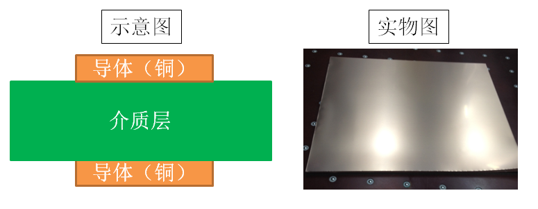
PCBs used in electronic products are basically composed of copper foil and organic materials, as shown in the figure below:
The copper foil we usually see appears very smooth on the surface, but in reality, it is not as smooth as the naked eye perceives. Copper foil is not completely smooth, as shown under a metallographic microscope in the figure below:

For easier understanding, a schematic diagram is provided below:
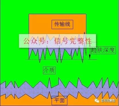
The surface of copper foil has numerous copper asperities. At present, there is no official data indicating the exact length of ordinary copper asperities (it varies by manufacturer). Based on the ordinary copper foil observed, the untreated copper asperities (copper foil roughness) are generally about 20~30μm. Of course, copper foil is conventionally classified into standard copper foil, reversed copper foil, low-roughness copper foil and ultra-low-roughness copper foil according to different roughness thickness (coefficient) values.
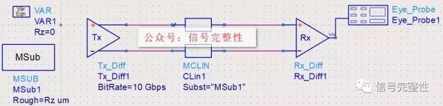
As mentioned earlier, copper foil roughness affects signal integrity, so let’s conduct an experiment to verify this. The schematic diagram is as follows: set copper foil roughness as a variable with an initial value of 0, and the simulation rate is 10Gbps:
Observe the eye diagram and waveform respectively, as shown below:
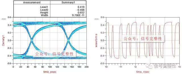
The results show that the eye diagram width is 97ps, the height is 0.652V, and the signal peak value is 0.479V.
Next, we gradually change the thickness of copper foil roughness to observe the changes in the eye diagram, and simulate the cases of copper foil roughness at 5μm, 10μm, 15μm and 20μm respectively. The eye diagrams and waveforms are as follows:
Copper Foil Roughness = 5μm
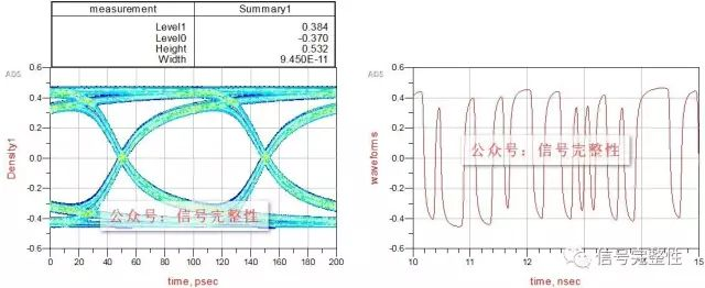
When the roughness is 5μm, the eye diagram width is 94.5ps and the height is 0.532V.
Copper Foil Roughness = 10μm
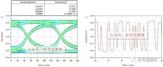
When the roughness is 10μm, the eye diagram width is 93ps and the height is 0.499V.
Copper Foil Roughness = 15μm
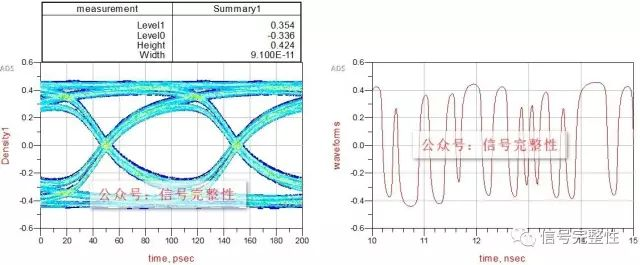
When the roughness is 15μm, the eye diagram width is 91ps and the height is 0.424V.
Copper Foil Roughness = 20μm
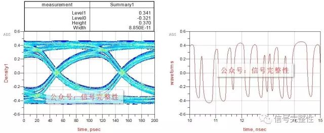
When the roughness is 20μm, the eye diagram width is 88.5ps and the height is 0.370V.
From the above results, we can see that as the copper foil roughness coefficient (thickness) increases, the eye diagram margin becomes smaller and the jitter becomes larger.
Many engineers often ask such a question: at what signal rate does the impact of copper foil roughness need to be considered in actual project engineering? My answer is that it is necessary to consider it at all times. However, considering the balance of cost and effect, when the signal rate exceeds 5Gbps, the selection of copper foil should be properly considered (it can be ignored if the design requirements are not high).
Therefore, as signal rates continue to rise, we need to pay attention not only to chip driving capability, PCB dielectric constant, dielectric loss angle, connectors, cables, etc., but also to the impact of the surface roughness of conductors (copper).
About Maxipcb
Maxipcb empowers innovators to turn cutting-edge technologies into reality.
We offer one-stop solutions for design, simulation, testing, PCB manufacturing, component procurement and SMT assembly, enabling efficient development, rapid deployment and risk control across the full product lifecycle.Serving the world in communications, industrial automation, aerospace, automotive, semiconductor and beyond, we build a safer, more connected future together.


 When the roughness is 5μm, the eye diagram width is 94.5ps and the height is 0.532V.
 When the roughness is 10μm, the eye diagram width is 93ps and the height is 0.499V.
 When the roughness is 15μm, the eye diagram width is 91ps and the height is 0.424V.
 When the roughness is 20μm, the eye diagram width is 88.5ps and the height is 0.370V.