During circuit schematic design, engineers typically define different GND ground lines as the 0V reference for various functional circuits to form independent current loops, thereby reducing mutual interference between circuits.
Introduction
During circuit schematic design, engineers typically define different GND ground lines as the 0V reference for various functional circuits to form independent current loops, thereby reducing mutual interference between circuits.
Classification of GND Ground Lines
-
Analog Ground (AGND)
Primarily used in analog circuits such as ADC acquisition circuits for analog sensors and operational amplifier scaling circuits.
-
Digital Ground (DGND)
Relative to AGND, it is used in digital circuits including key detection circuits, USB communication circuits, and MCU circuits.
-
Power Ground (PGND)
AGND and DGND are for low-power circuits, while a separate PGND serves as the reference ground for high-power circuits like motor drive circuits and solenoid valve drive circuits.
-
Power Supply Ground (GND)
AGND, DGND and PGND all fall into the category of DC ground lines, and they ultimately converge to form the universal 0V reference ground for the entire circuit, namely the power supply ground (GND).
-
AC Ground (CGND)
Generally used in circuits with AC power supplies, such as AC-DC power conversion circuits.
-
Earth Ground (EGND)
The ground connected to the physical earth for electrical safety and noise suppression.
The Rationale Behind Segmented GND
Why are there so many types of GND, and why is segmentation necessary? Many engineers simply label all grounds as GND in schematics without differentiation, leading to direct connection of all ground lines during PCB routing. This seemingly convenient practice causes a series of issues:
-
Signal Crosstalk
Direct connection of grounds for different functions allows high-power circuits to interfere with the 0V reference of low-power circuits through the ground line, resulting in crosstalk between different circuit signals.
-
Signal Accuracy Degradation
Accuracy is the core performance index of analog circuits—without it, analog circuits lose their intended function. Unlike stable DC ground (0V), AC ground (CGND) has a sinusoidal, periodically fluctuating voltage. Connecting CGND with analog ground (AGND) causes AGND to fluctuate with CGND, compromising the voltage accuracy of analog signals.
-
EMC Test Failures
Electromagnetic radiation (EMC) intensity correlates with signal strength. Merging different grounds lets the strong-signal circuit’s ground interfere with the weak-signal one, turning the weak-signal circuit into a strong EMC radiation source and increasing the difficulty of passing EMC tests.
-
Reduced Circuit Reliability
Circuits with fewer interconnections have stronger independent operation capabilities. Merging grounds of different functional circuits creates an interference link between them, significantly reducing the overall reliability of the circuit system.
Step-by-Step Guide to Routing GND on PCBs
GND is as critical to a PCB as water is to the human body. Follow these key principles to route GND effectively:
1. Implement Ground Segmentation by Function
Different functional modules on a PCB have distinct GND requirements. Improper merging of power ground and signal ground is a common mistake.
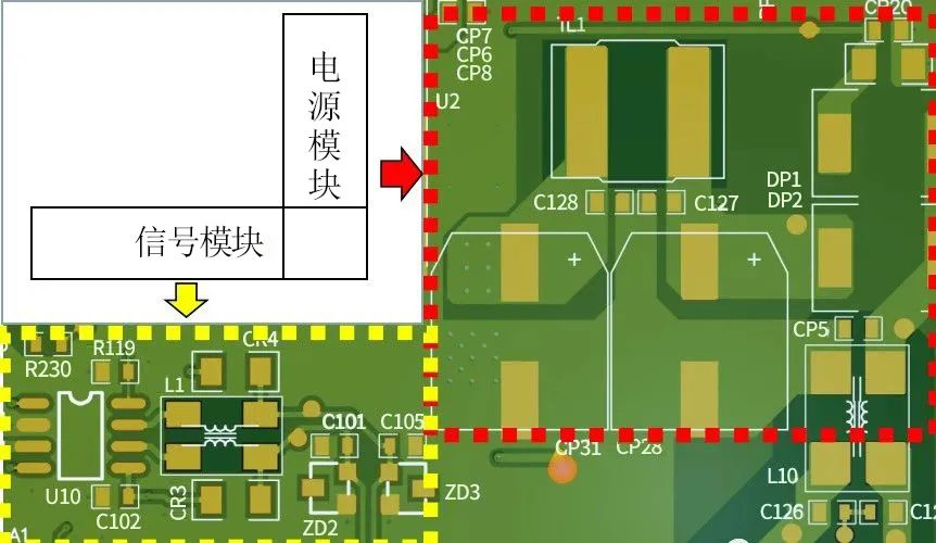
PCB layout with conflicting power ground and signal ground
In the layout above, the power module’s GND acts as the
power negative terminal (not a true 0V reference), while the signal module’s GND is the
0V reference ground. Noise on the power ground directly interferes with the signal module.
Solutions:
- Separate the signal ground from the power ground and avoid direct connection.
- Isolate the signal ground area; if power supply is needed, use dedicated traces for power delivery instead of shared ground.
2. Avoid Disrupted (Stepped) GND Planes
Structural constraints may split a single module’s intended continuous GND plane into multiple segments with traces crossing through—this is called a
stepped GND.
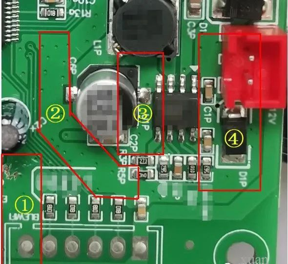
PCB layout with stepped GND on a power module
In the example above, the power input negative terminal (GND at position ①) is separated from position ② by signal traces, ② from ③ by 5V output traces, and ③ from ④ by a chip enable trace. While a multimeter may show electrical continuity, this layout is unreasonable in terms of signal path order and
high-frequency ground impedance. For power modules (a major source of EMC issues), the GND plane
must be continuous on the same layer.
3. Reject "Waist-shaped" and "Pigtail-shaped" GND
When pouring copper for GND on a PCB, traces or vias may create narrow "waist-shaped" connections between GND regions, or thin "pigtail-shaped" GND stubs.
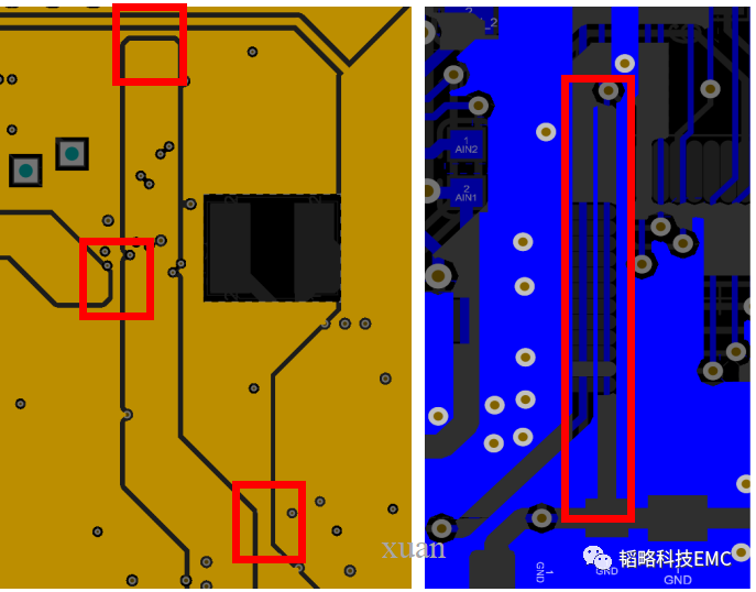
Left: Waist-shaped GND; Right: Pigtail-shaped GND
Both layouts severely degrade EMI and EMS performance.
Solutions:
- Widen the narrow sections of waist-shaped GND, or stop copper pouring in overly small areas entirely.
- Cut off pigtail-shaped GND stubs; if the area is functionally necessary, add more vias to ensure reliable grounding.
Conclusion
Routing GND on a PCB requires repeated checks and global layout planning—never cut corners for convenience or ground a node just for the sake of it. When pouring GND copper, always:
- Verify if different functional GND regions can be connected directly.
- Check for unreasonable GND paths among dense traces.
- Confirm the actual function of GND in each circuit region.
About Maxipcb
Maxipcb empowers innovators to turn cutting-edge technologies into reality.
We offer one-stop solutions for design, simulation, testing, PCB manufacturing, component procurement and SMT assembly, enabling efficient development, rapid deployment and risk control across the full product lifecycle.Serving the world in communications, industrial automation, aerospace, automotive, semiconductor and beyond, we build a safer, more connected future together.


