Decoupling capacitors (also called bypass capacitors) are placed near the power pins of components to filter high-frequency noise, stabilize voltage, and ensure normal operation.
What Are Decoupling Capacitors and Why Do We Need Them?
1. Introduction
Decoupling capacitors (also called bypass capacitors) are placed near the power pins of components to filter high-frequency noise, stabilize voltage, and ensure normal operation.
2. Analysis
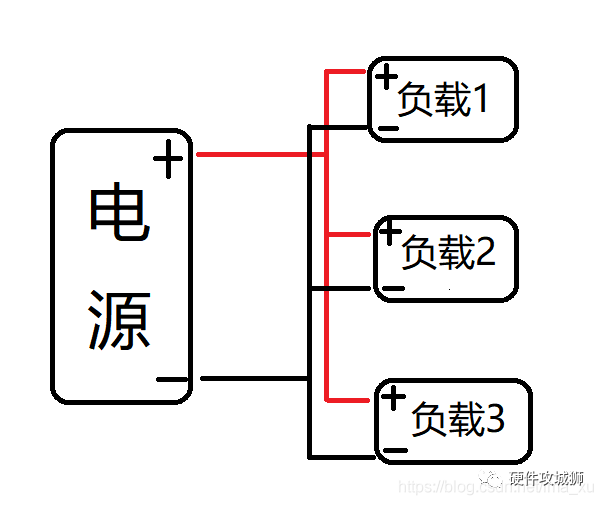
A circuit system usually has multiple loads sharing the same power supply.
Ideal power supply waveform for a load:
In reality, loads dynamically draw current, causing unstable supply voltage:
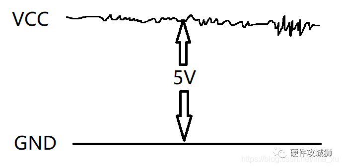
Actual noisy power supply waveform (5V DC with high-frequency AC noise)
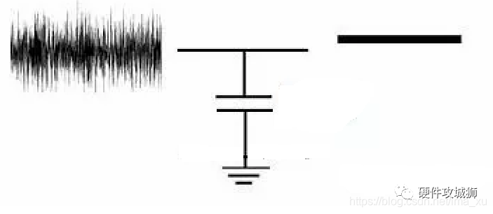
The AC noise coupled onto the DC rail disrupts both the local load and other devices on the same power rail.
The solution is to
place a small capacitor in parallel across the power rails.
Before vs. after adding decoupling capacitor – noisy waveform becomes clean
The capacitor bypasses high-frequency noise to ground, leaving clean DC power. We should add one decoupling capacitor per load, plus input filtering capacitors at the power input.
How to Choose Decoupling Capacitors
Common questions:
- What capacitance value works best?
- Which type should I use?
- Why do we use multiple capacitors of different values on one power pin?
Analysis
A chip (FPGA/MCU) needs parallel capacitors of different values and types for effective decoupling.
All capacitors have three key parameters:
- Capacitance supplies transient current
- ESR (Equivalent Series Resistance): constant impedance vs. frequency
- ESL (Equivalent Series Inductance): impedance rises with frequency
Ceramic capacitors: very low ESR/ESL, low cost – best for high frequencies.
Tantalum capacitors: moderate ESR/ESL, high capacitance density – good for low-frequency compensation.
Larger packages usually have higher ESL.
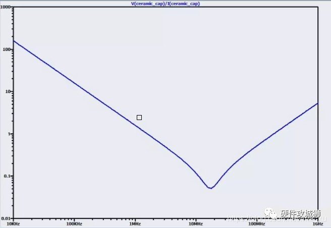
Impedance vs. frequency curve for 0.1μF 0603 ceramic capacitor (ESL=850pH, ESR=50mΩ)
Due to ESL, impedance reaches a minimum at the self-resonant frequency and then rises.
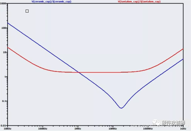
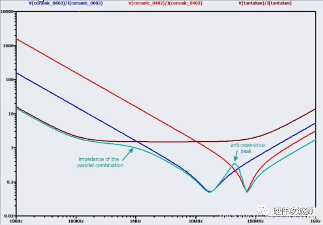
Impedance comparison between 1μF tantalum and 0.1μF ceramic capacitor
Tantalum has lower impedance at very low frequencies but becomes much worse above ~1MHz. For 10MHz noise, a small ceramic capacitor performs far better.
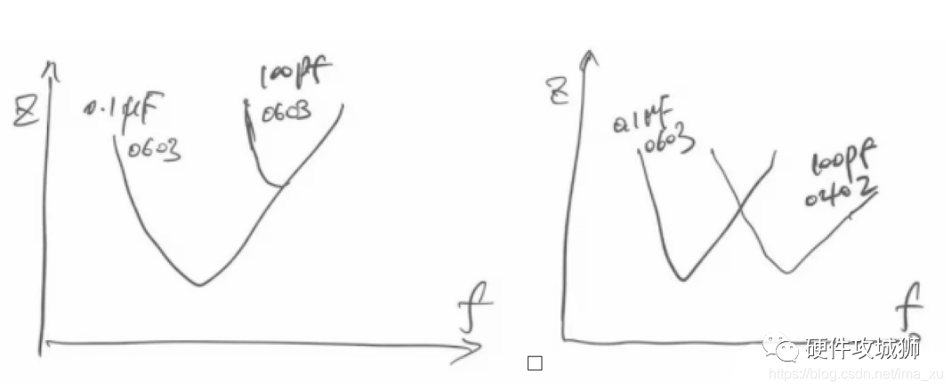
Left: two same-package capacitors in parallel; Right: 0.1μF 0603 + 100pF 0402 covering wider frequency range
Typical combination for one power pin:
- 4.7μF tantalum: filters low-frequency noise
- 0.1μF 0603 ceramic: effective for 1–50MHz
- 0.001μF 0402 ceramic: effective above 50MHz
Rules of thumb:
- Ceramic > electrolytic for high-frequency decoupling
- Smaller capacitance → higher self-resonant frequency
- Smaller package → higher self-resonant frequency
PCB Layout & Routing for Decoupling Capacitors
1. Principles
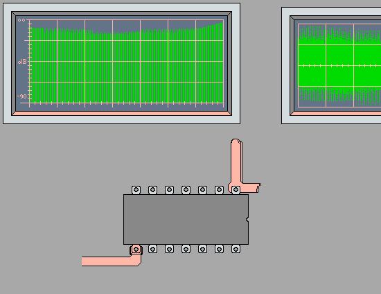
Animation showing how placement distance drastically affects decoupling performance
Key takeaways:
- A 0.1μF (104) capacitor near the power pin suppresses noise effectively
- Power → Capacitor → Ground path must be as short as possible
- For high-frequency decoupling, 0.01μF, 0.1μF, 1μF (same package) perform similarly
- SMD capacitors perform much better than through-hole (lower lead inductance)
- Solid power and ground planes shorten paths and act as a large parallel capacitor
2. Examples
In an STM32F103C8T6 minimum system, four decoupling capacitors serve the four power-pin pairs.
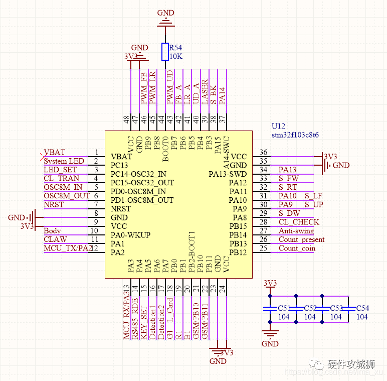
STM32 with decoupling capacitors placed close to the MCU
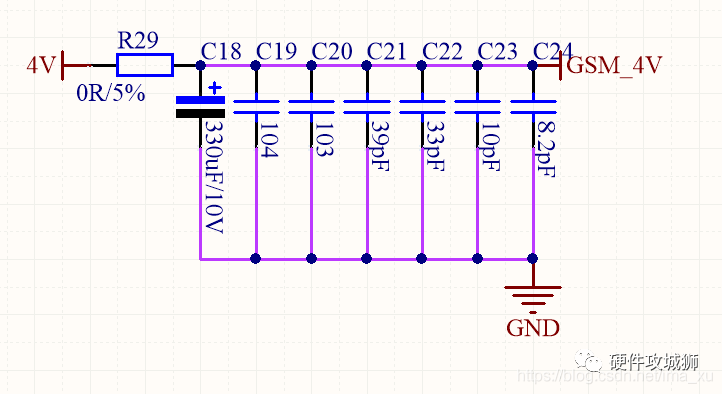
For sensitive applications (e.g., GSM power), use multiple capacitors:
GSM power section with 6+1 decoupling capacitors
Placement rule: smaller capacitors closer to the IC; larger capacitors farther away.
- C24 (8.2pF): closest to GSM
- C19 (100nF): medium distance
- 330μF tantalum: farthest
3. Summary
Comparison of via-to-ground connection methods (from worst to best)
Complete PDN (Power Distribution Network) showing capacitor hierarchy from die to system power
One-sentence rule:
Decoupling capacitor layout must
minimize parasitic resistance and inductance.
About Maxipcb
Maxipcb empowers innovators to turn cutting-edge technologies into reality.
We offer one-stop solutions for design, simulation, testing, PCB manufacturing, component procurement and SMT assembly, enabling efficient development, rapid deployment and risk control across the full product lifecycle.Serving the world in communications, industrial automation, aerospace, automotive, semiconductor and beyond, we build a safer, more connected future together.