Although many converters feature tri-state outputs/inputs, the associated registers are still on-chip. These can couple data pin signals into sensitive areas, making isolation buffers a sound design practice. In some cases, additional data buffers must be placed directly at the converter output on the analog ground plane for enhanced isolation.
Introduction
Although many converters feature tri-state outputs/inputs, the associated registers are still on-chip. These can couple data pin signals into sensitive areas, making isolation buffers a sound design practice. In some cases, additional data buffers must be placed directly at the converter output on the analog ground plane for enhanced isolation.
Placing data buffers close to the converter effectively isolates digital outputs from data bus noise (Figure 1). Buffers also minimize loading on the converter’s digital outputs and provide a Faraday shield between the digital outputs and the data bus (Figure 2).
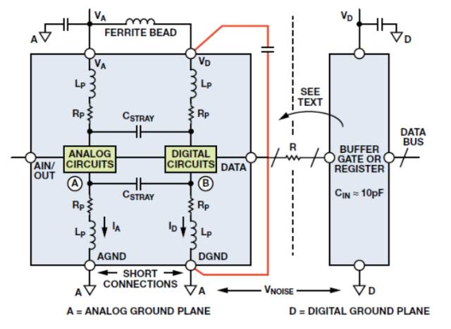
Figure 1 – Proper grounding for mixed-signal ICs with low internal digital current
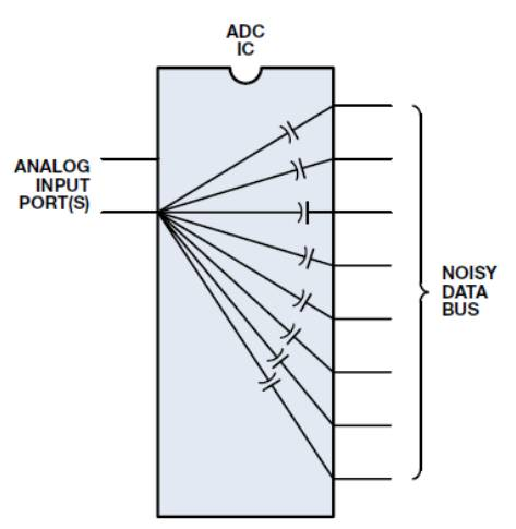
Figure 2 – High-speed ADC with output buffers/latches for enhanced immunity to digital data bus noise
A series resistor (marked "R" in Figure 1) between the ADC output and buffer register input helps minimize digital transient currents that could degrade converter performance. This resistor decouples the digital output driver from the buffer register input capacitance. Additionally, the RC network formed by the series resistor and input capacitance acts as a low-pass filter to slow fast signal edges.
A typical CMOS gate, combined with PCB traces and vias, creates a load of approximately 10 pF. Without an isolation resistor, a logic output with a 1 V/ns slew rate generates a 10 mA dynamic current.
A 500 Ω series resistor driving a 10 pF register input capacitance minimizes transient output current and produces a rise/fall time of approximately 11 ns:
tr=2.2×R×C=2.2×500 Ω×10 pF=11 nsTTL registers should be avoided due to their higher input capacitance, which significantly increases dynamic switching current.
Buffer registers and other digital circuits must be grounded and decoupled to the PCB’s digital ground plane. Note that any noise between the analog and digital ground planes can reduce the noise margin on the converter’s digital interface. Since digital noise immunity is at the hundreds or thousands of millivolts level, this is generally not a critical issue. Analog ground plane noise is typically low, but if noise on the digital ground plane (relative to the analog ground plane) exceeds several hundred millivolts, measures should be taken to reduce digital ground plane impedance to maintain an acceptable noise margin. Under no circumstances should the voltage between the two ground planes exceed 300 mV, as this may damage the IC.
Power Supply and Decoupling
It is best to provide separate power supplies for analog and digital circuits. The analog power supply should power the converter. If the converter has a dedicated digital power pin (VD), it should be powered by the independent analog supply or filtered as shown in Figure 3. All converter power pins must be decoupled to the analog ground plane, and all logic circuit power pins to the digital ground plane (Figure 3). The digital power supply can power analog circuits only if it is exceptionally quiet, and extreme caution is required in such cases.
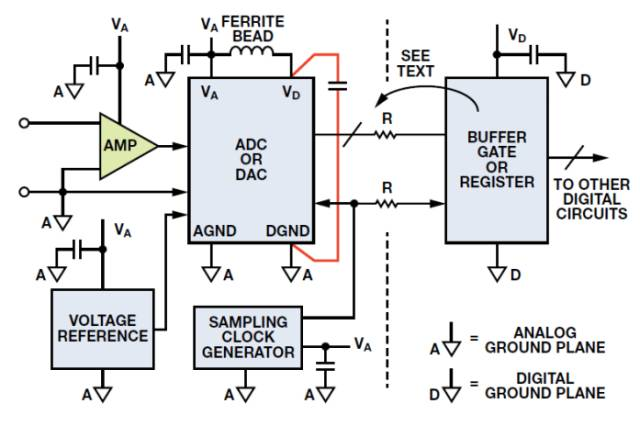
Figure 3 – Grounding and decoupling points for ADC systems
In some cases, connecting VD to the analog power supply is not feasible. Some high-speed ICs use a +5 V supply for analog circuits and a +3.3 V (or lower) supply for the digital interface to match external logic. In this scenario, the IC’s +3.3 V pin should be decoupled directly to the analog ground plane. A ferrite bead is also recommended in series with the power trace to connect the pin to the +3.3 V digital logic supply.
The sampling clock generation circuit should be treated the same as analog circuits: grounded and heavily decoupled to the analog ground plane.
Grounding for High-Frequency Operation
It is generally recommended that power and signal currents return through a ground plane, which also serves as a reference node for the converter, voltage reference, and other subcircuits. However, even extensive use of a ground plane does not guarantee a high-quality ground reference for AC circuits.
Figure 4 shows a simple circuit on a two-layer PCB with an AC/DC current source on the top layer, connected to Via 1 at one end and Via 2 via a U-shaped copper trace at the other. Both vias pass through the board to the ground plane. Ideally, the impedance in the ground loop between the top connector, Via 1, and Via 2 is zero, resulting in zero voltage across the current source.
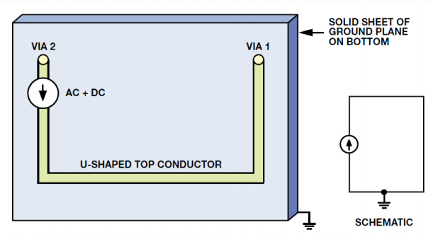
Figure 4 – Schematic and layout of a current source with a U-shaped trace on a PCB, returning through the ground plane
This simple schematic hides inherent subtleties, but understanding how current flows from Via 1 to Via 2 in the ground plane reveals practical issues and solutions for eliminating grounding noise in high-frequency layouts.
DC vs. AC Current Paths in the Ground Plane
DC current flows along the path of minimum resistance from Via 1 to Via 2 in the ground plane (Figure 5). While some current spreading occurs, the path deviates little from this direct route. In contrast, AC current follows the path of minimum impedance, which is determined by inductance at high frequencies.
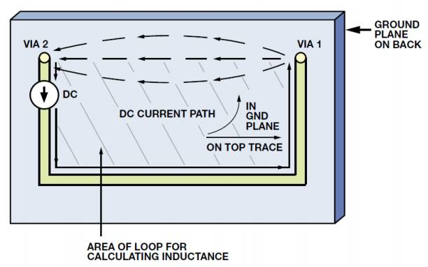
Figure 5 – DC current flow in the PCB ground plane for the circuit in Figure 4
Inductance is proportional to the area of the current loop, a relationship illustrated by the right-hand rule and magnetic fields in Figure 6. Inside the loop, magnetic fields generated by current flowing along all parts of the loop reinforce each other; outside the loop, fields from different parts cancel out. Thus, the magnetic field is essentially confined within the loop. A larger loop means higher inductance, which stores more magnetic energy (Li2) for a given current, has higher impedance (XL=jωL), and produces a larger voltage at a given frequency.
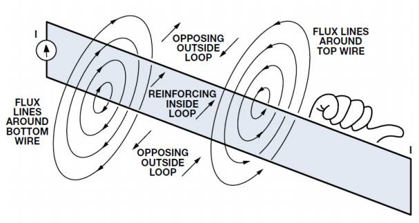
Figure 6 – Magnetic field lines and inductive loops (right-hand rule)
AC current naturally takes the path of lowest impedance in the ground plane. Ignoring resistance, high-frequency AC current flows along the path that forms the smallest enclosed area with the U-shaped top trace.
In the example shown, the smallest loop is clearly formed by the U-shaped top trace and the portion of the ground plane directly beneath it. Figure 7 shows the AC current path in the ground plane (minimal enclosed area, directly below the U-shaped top trace), in contrast to the DC path in Figure 5. In practice, ground plane resistance causes low-to-mid frequency current to flow somewhere between the direct return path and the area beneath the top trace. However, even at frequencies as low as 1–2 MHz, the return path is close to the underside of the top trace.
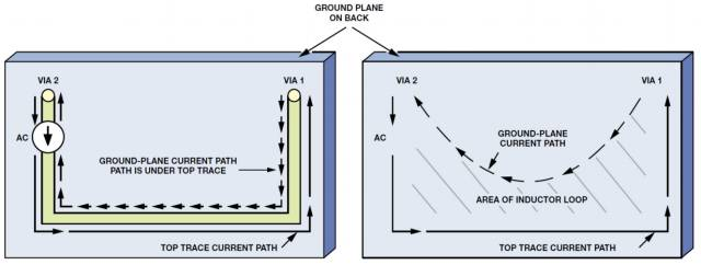
Figure 7 – AC current paths in the ground plane: resistance-free (left) and with resistance (right)
Sampling Clock Considerations
In high-performance sampled-data systems, a low-phase-noise crystal oscillator should generate the ADC (or DAC) sampling clock. Sampling clock jitter modulates the analog input/output signal, increasing the noise and distortion floor. The sampling clock generator must be isolated from high-noise digital circuits and grounded/decoupled to the analog ground plane, the same as op-amps and ADCs.
The impact of sampling clock jitter on ADC signal-to-noise ratio (SNR) can be approximated by the following formula:
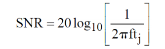
SNR degradation due to sampling clock jitter
where f is the analog input frequency, and tj is the rms sampling clock jitter. For example, if tj=50 ps (rms) and f=100 kHz, the SNR is 90 dB, equivalent to a dynamic range of approximately 15 bits.
Note that tj in the example is the root-sum-square (RSS) of external clock jitter and internal ADC clock jitter (aperture jitter). In most high-performance ADCs, internal aperture jitter is negligible compared to jitter on the sampling clock.
Since SNR degradation is primarily caused by external clock jitter, measures must be taken to make the sampling clock as noise-free as possible with the lowest possible phase jitter—requiring the use of a crystal oscillator. Many manufacturers offer small crystal oscillators with CMOS-compatible outputs and low jitter (<5 ps rms).
Ideally, the sampling clock crystal oscillator should reference the analog ground plane in a separate grounding system. However, system constraints may prevent this. In many cases, the sampling clock must be derived from a higher-frequency, multi-purpose system clock generated on the digital ground plane and then transmitted to the ADC on the analog ground plane. Ground noise between the two planes is directly added to the clock signal, causing excessive jitter—which degrades SNR and generates interfering harmonics.
This issue can be mitigated by transmitting the sampling clock as a differential signal using a small RF transformer (Figure 8) or high-speed differential drivers/receivers. If the latter is used, ECL logic is preferred to minimize phase jitter. In a single +5 V supply system, ECL logic can be biased between ground and +5 V (PECL), with the output AC-coupled to the ADC sampling clock input. In all cases, the original master system clock must be generated from a low-phase-noise crystal oscillator.
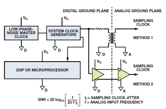
Figure 8 – Sampling clock distribution between digital and analog ground planes
About Maxipcb
Maxipcb empowers innovators to turn cutting-edge technologies into reality.
We offer one-stop solutions for design, simulation, testing, PCB manufacturing, component procurement and SMT assembly, enabling efficient development, rapid deployment and risk control across the full product lifecycle.Serving the world in communications, industrial automation, aerospace, automotive, semiconductor and beyond, we build a safer, more connected future together.


