In the design of high-speed analog signal chain, the layout of printed circuit board (PCB) needs to consider many options, some of which are more important than others, while others depend on the application. The final answer is different, but in all cases, the design engineer should try to eliminate the error of best practices and not care too much about every detail of layout and wiring.
In the design of high-speed analog signal chain, the layout of printed circuit board (PCB) needs to consider many options, some of which are more important than others, while others depend on the application. The final answer is different, but in all cases, the design engineer should try to eliminate the error of best practices and not care too much about every detail of layout and wiring.
Exposed padThe exposed pad (EPAD) is sometimes ignored, but it is very important to give full play to the performance of the signal chain and to fully dissipate heat of the device.
The exposed pad, which ADI calls Pin 0, is the pad under most devices at present. It is an important connection, through which all internal grounding of the chip is connected to the center point below the device. I wonder if you have noticed that many converters and amplifiers lack grounding pins at present, and the reason is the exposed pads.
The key is to properly fix (i.e. solder) this pin to the PCB, so as to achieve a reliable electrical and thermal connection. If this connection is not strong, confusion will occur, in other words, the design may be invalid.
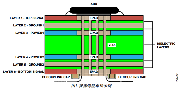
Achieve the best connectionThere are three steps to achieve the best electrical and thermal connection using exposed pads. First of all, if possible, the exposed pads should be copied on each PCB layer. The purpose of this is to form a dense thermal connection with all grounding and grounding layers, so as to quickly dissipate heat. This step is related to high-power devices and applications with high channel count. Electrically, this will provide a good equipotential connection for all grounding layers.
You can even copy the exposed pad on the bottom layer (see Figure 1), which can be used as a ground point for decoupling heat dissipation and a place to install the bottom radiator.
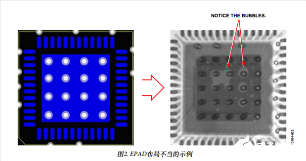
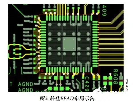
Secondly, the exposed pad is divided into several identical parts, like a chessboard. Use a screen cross grid on the open exposed pad, or use a solder mask. This step can ensure a stable connection between the device and the PCB. In the assembly process of reflow soldering, it is impossible to determine how the solder paste flows and finally connect the device with PCB.
Connections may exist, but they are unevenly distributed. You may only get one connection, and the connection is small, or worse, it is located at the corner. Dividing the exposed pad into smaller parts can ensure that there is a connection point in each area, and realize a more secure and uniform connection of the exposed pad (see Figure 2 and Figure 3).
Finally, you should ensure that all parts have vias connected to the ground. Each area is usually large enough to accommodate multiple vias. Before assembly, it is very important to fill each via with solder paste or epoxy resin, which can ensure that the solder paste on the exposed pad will not flow back into these via holes and affect the correct connection. Finally, you should ensure that all parts have vias connected to the ground. Each area is usually large enough to accommodate multiple vias. Before assembly, it is very important to fill each via with solder paste or epoxy resin, which can ensure that the solder paste on the exposed pad will not flow back into these via holes and affect the correct connection.
Decoupling and layer capacitanceSometimes engineers will ignore the purpose of decoupling and just disperse many capacitors with different sizes on the circuit board to connect the lower impedance power supply to the ground. But the question remains: how much capacitance is needed? Many related literatures show that many capacitors with different sizes must be used to reduce the impedance of power transmission system (PDS), but this is not completely correct. On the contrary, PDS impedance can be reduced only by selecting the correct size and kind of capacitor.
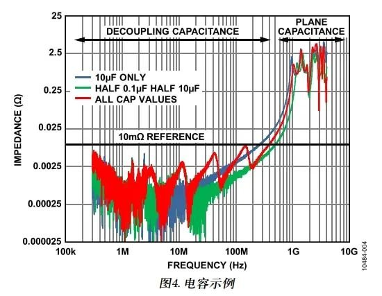
For example, consider designing a 10 mΩ reference layer, as shown in Figure 4. As shown in the red curve, many capacitors with different values are used on the system circuit board, such as 0.001 μF, 0.01 μF, 0.1 μF and so on. This can certainly reduce the impedance in the frequency range of 500 MHz, but if you look at the green curve, the same design only uses 0.1 μF and 10 μF capacitors. This proves that if the correct capacitors are used, so many capacitors are not needed. This also helps to save space and BOM costs.
Note that not all capacitors are "created equal", and even the same supplier has different processes, sizes and styles. If the correct capacitor is not used, whether it is multiple capacitors or several different types, it will bring adverse effects to PDS.
The result may be an inductive loop. Misplaced capacitors or capacitors of different technologies and models (thus responding differently to the frequency in the system) may resonate with each other (see Figure 5).
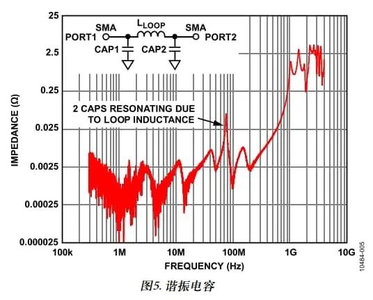
It is important to know the frequency response of the type of capacitor used in the system. The efforts to design a low impedance PDS system will be wasted if the capacitors are chosen at will.
High frequency layer capacitance of PDSTo design a qualified PDS, it is necessary to use various capacitors (see Figure 4). Typical capacitance values used on PCB can only reduce the impedance of DC or near DC frequency to about 500 MHz. Above 500 MHz, the capacitance depends on the internal capacitance formed by PCB. Note that it is helpful to closely overlap the power plane and the ground plane.
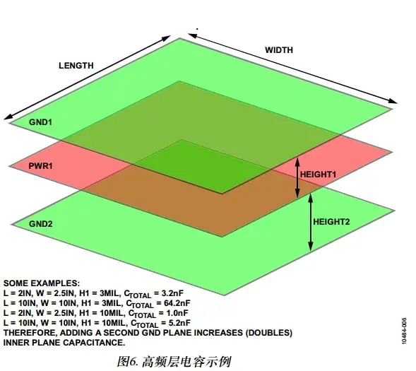
We should design a PCB laminated structure that supports larger layer capacitance. For example, a six-layer stack may include a top signal layer, a first ground layer, a first power layer, a second power layer, a second ground layer and a bottom signal layer. It is stipulated that the first ground layer and the first power layer are close to each other in the laminated structure, and the distance between the two layers is 2 to 4 mils, forming an inherent high-frequency layer capacitance. The biggest advantage of this capacitor is that it is free, just note it in PCB manufacturing notes. If the power plane must be divided and there are multiple VDD power rails on the same plane, the largest power plane should be used. Don't leave holes, and pay attention to sensitive circuits. This will maximize the capacitance of the VDD layer.
If the design allows additional layers (in the above example, from six to eight), two additional ground layers should be placed between the first and second power layers. When the core spacing is also 2 to 3 mils, the inherent capacitance of the laminated structure will be doubled at this time (see Figure 6 for an example).
This structure is easier to design than adding more discrete high-frequency capacitors to keep low impedance at high frequencies.
The task of PDS is to minimize the voltage ripple in response to the power supply current demand, which is important but often overlooked. All circuits need current, some circuits need more current, and some circuits need to provide current at a faster rate. It is helpful to minimize the voltage ripple caused by the current demand of the circuit by adopting a fully decoupled low impedance power supply layer or ground layer and a good PCB stack. For example, according to the decoupling strategy used, if the switching current of the system is 1 A and the impedance of PDS is 10 mω, the maximum voltage ripple is 10 mV. The calculation is simple: V = IR.
With the perfect PCB stack, the high frequency range can be covered, and the low frequency range (< 500 MHz) can be covered by using traditional decoupling around the initial entry point of the power layer and high power or surge current devices. This ensures that the PDS impedance is the lowest in the whole frequency range. There is no need to configure capacitors everywhere; Placing the capacitor right against each IC will break many manufacturing rules. If such drastic measures are needed, there are other problems in the circuit.
Layer couplingSome layouts inevitably have overlapping circuit layers (see fig. 8). In some cases, it may be a sensitive analog layer (such as power supply, grounding or signal), and the lower layer is a high-noise digital layer.
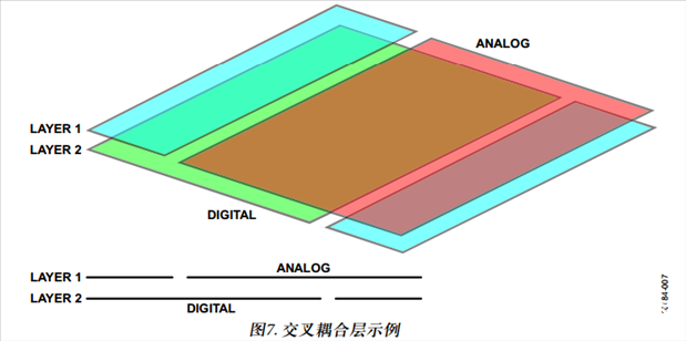
This is often overlooked because the high noise layer is on another layer-below the sensitive analog layer. However, a simple experiment can prove this is not the case. Take a certain layer as an example, and inject signals into any layer. Then another layer is connected, and the adjacent layer is cross-coupled to the spectrum analyzer. The amount of signals coupled to adjacent layers is shown in fig. 8. Even if the spacing is 40 mils, it is still a capacitor in a sense, so it will still couple signals to adjacent layers at some frequencies.
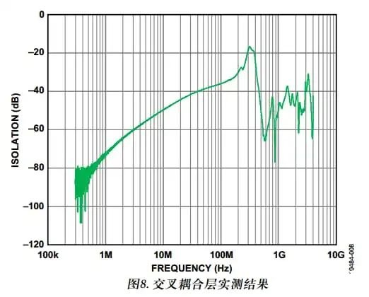
Figure 8 shows an example of this. For example, suppose that a high-noise digital layer on one level has a 1 V signal that is switched at high speed. This means that the other layer will see 1 mV coupling (about 60 dB isolation). For a 12-bit ADC with 2-V p-p full-scale swing, this is 2 LSB coupling. This may not be a problem for a specific system, but it should be noted that if the sensitivity of the system is increased by two bits, from 12 bits to 14 bits, the sensitivity of this coupling will only be increased by four times, that is, 8 LSB.
Ignoring this type of cross-layer coupling may invalidate the system or weaken the design. It must be noted that the coupling between the two layers may be beyond imagination.
Attention should be paid to this when noise stray coupling is found in the target spectrum. Sometimes the layout determines that unexpected signals or layers should be cross-coupled to different layers. Similarly, you should pay attention to this when debugging sensitive systems. The problem may appear on the next floor.
Separate groundingThe most common question that analog signal chain designers ask is: Should the ground plane be divided into AGND and DGND when using ADC? The short answer is: it depends.
The detailed answer is: usually not separated. Why not? Because in most cases, blindly separating the ground plane will only increase the inductance of the return path, which will do more harm than good.
It can be seen from the formula V = L(di/dt) that the voltage noise will increase with the increase of inductance. With the increase of inductance, the PDS impedance that designers have been trying to keep down will also increase. As the demand for increasing the sampling rate of ADC continues to grow, there are limited ways to reduce the switching current (di/dt). Therefore, unless it is necessary to separate the ground plane, please keep these ground connections.
The key is to divide the circuit reasonably, so there is no need to separate the ground plane, as shown in Figure 9. Note that there is no need to separate the ground plane if the layout allows you to keep the circuits in their respective areas. This division can provide star grounding, thus limiting the return current to specific circuit parts.
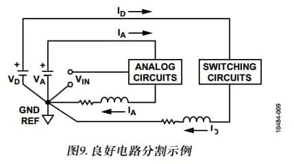
For example, due to the size limitation, when the circuit board cannot achieve good layout division, it is necessary to separate the ground plane. This may be because in order to meet the traditional design requirements or dimensions, messy bus power supplies or high-noise digital circuits must be placed in some areas. In this case, separating the ground plane is the key to achieve good performance. However, in order to make the overall design effective, these ground planes must be connected together by a bridge or connection point somewhere on the circuit board. Therefore, the connection points should be evenly distributed on the separated ground plane.
In the end, there is often a connection point on the PCB that becomes the best place for the return current to pass through without causing performance degradation or forcibly coupling the return current to the sensitive circuit. If this connection point is located at, near or below the converter, there is no need to separate the ground.
Concluding remarksBecause there are too many best options, layout considerations are always confusing. Technology and principles have always been part of the company's design culture. Engineers like to learn from previous design experience, and the pressure of product listing makes designers reluctant to change or try new technologies. They stick to the risk balance until there is a major problem in the system.
At the evaluation board, module and system level, simple single grounding is the best. Good circuit division is the key. This also affects the layout of layers and adjacent layers. If the sensitive layer is above the noisy digital layer, please be aware that cross-coupling may occur. Assembly is also important; The manufacturing notes provided to PCB workshop or assembly workshop should be made good use of to ensure a reliable connection between IC exposed pads and PCB.
Poor assembly often leads to poor system performance. Decoupling near the power plane entry point and the VDD pin of the converter or IC is always beneficial. However, in order to increase the inherent high-frequency decoupling capacitance, closely stacked power and ground layers (spacing ≤4 mils) should be used. This method will not bring extra cost, just take a few minutes to update PCB manufacturing notes.
When designing the layout of high-speed and high-resolution converters, it is difficult to take care of all the specific characteristics. Every application is unique. It is hoped that the points mentioned in this application note will help design engineers to better understand the future system design.
About Maxipcb
Maxipcb empowers innovators to turn cutting-edge technologies into reality.
We offer one-stop solutions for design, simulation, testing, PCB manufacturing, component procurement and SMT assembly, enabling efficient development, rapid deployment and risk control across the full product lifecycle.
Serving the world in communications, industrial automation, aerospace, automotive, semiconductor and beyond, we build a safer, more connected future together.


