On the basis of this circuit, how to suppress ringing without adjusting the frequency of excitation source and the values of L and C?
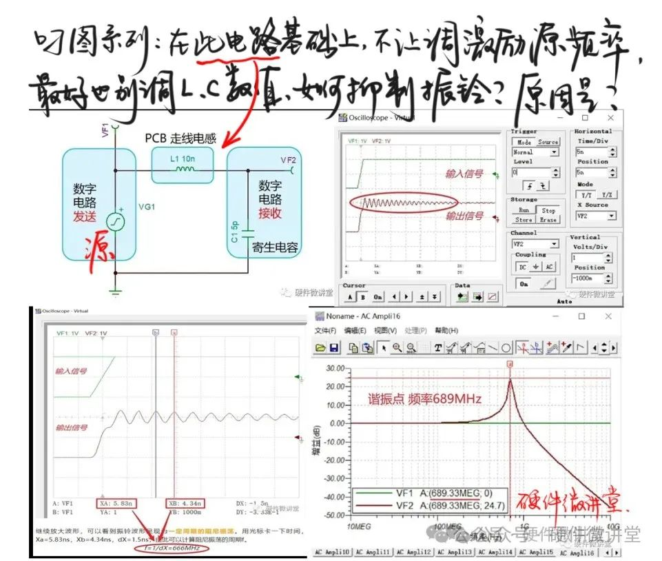
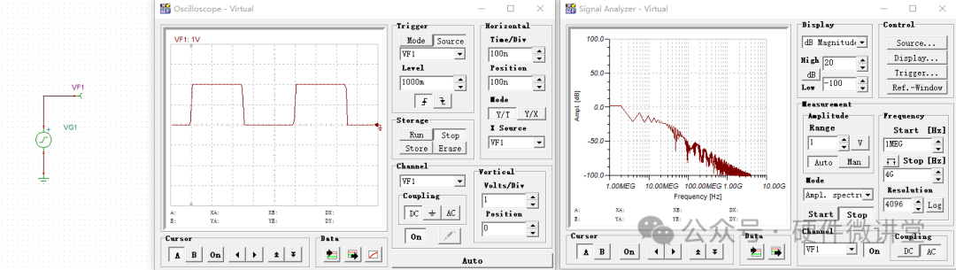
In the picture, the excitation source VG1 is a square wave of 2MHz. After L1 and C1, the edge of the output terminal VF2 rings obviously. On the basis of this circuit, how to suppress ringing without adjusting the frequency of excitation source and the values of L and C?
This problem is very common in the debugging of real problems. We often encounter that the PCB has been completed and the board has been pasted. The power-on test found that the waveform of a driving signal was poor and there was obvious ringing. What should we do?
① Adjust the circuit parameters; -> to change the BOM, the pasted boards must be reworked and restructured;
(2) adding a ringing suppression circuit; -> to change the PCB, re-board, wasting time and money;
③ frequency reduction; -> reducing the frequency of excitation source is a common means of SI debugging, but the actual conditions may not allow it. The frequency is usually planned in advance in the design stage, and the whole body will be moved by pulling one hair.
None of this works. What should we do? Today, let's discuss ...
Frequency spectrum of excitation source
The excitation source we used in the previous simulation is a square wave of 2MHz with a rising edge of 2ns. We still use TINA-TI for simulation, and choose "oscilloscope" to look at the time domain signal of the excitation source and "signal analyzer" to look at the frequency spectrum of the signal. The simulation results are shown in the following figure:

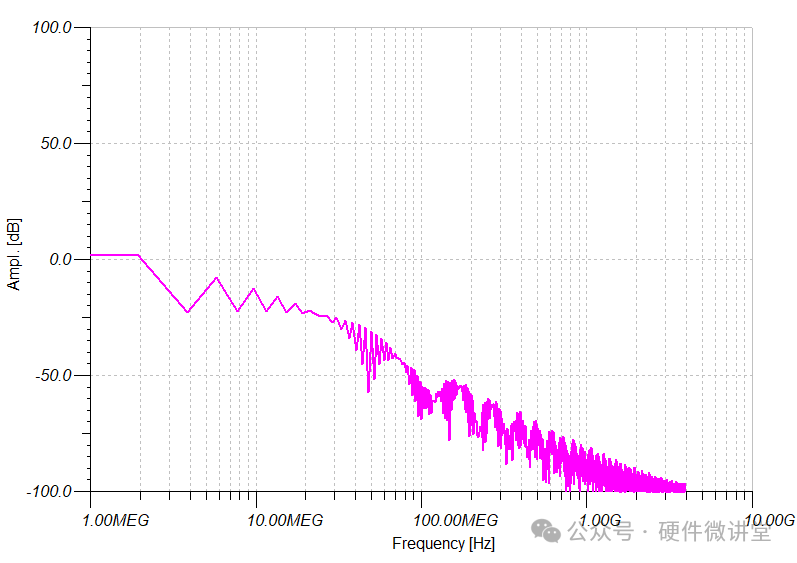
Let's take a look at the picture of the spectrum separately.
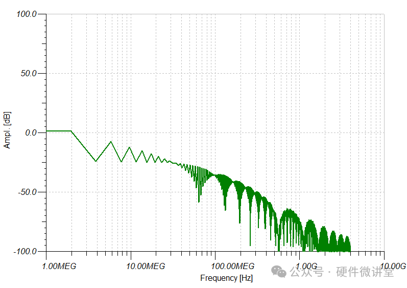
Maybe you can't see anything just by looking at this picture. Let's mark two sets of data.
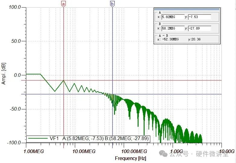
The first group: the cursor A is 5.82MHz, and the corresponding amplitude is-7.53 dB; The cursor B is 58.2MHz, and the corresponding amplitude is -27.89dB, with a difference of about 20dB.
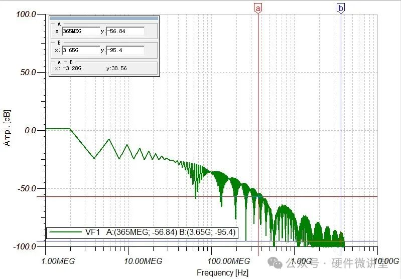
The second group: the cursor A is 365MHz, and the corresponding amplitude is-56.84 dB; The cursor B is 3.65GHz, and the corresponding amplitude is -95.4dB, with a difference of about 40dB.
Speaking of which, some students may remember something. That's right, it's the envelope asymptote of trapezoidal wave spectrum. The square wave in reality will not be an ideal square wave, and there will be a certain rising edge and falling edge. Even if it is ns level or ps level, it can still be regarded as a trapezoidal wave. Therefore, understanding the envelope asymptote of trapezoidal wave spectrum has a wide guiding significance.
Spectral envelope asymptote of trapezoidal wave
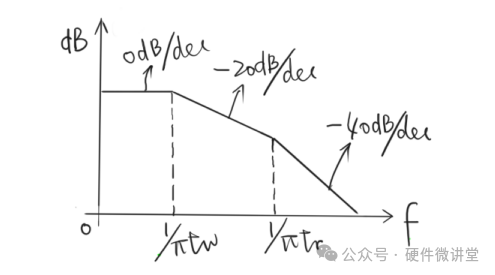
The spectral envelope of trapezoidal wave is surrounded by three asymptotes and two demarcation points:
① Asymptote 0dB/10dec: within the range of 0~f1;
② Asymptote -20dB/10dec: in the range of f1~f2;
③ Asymptote -40dB/10dec: in the range greater than f2;
④ demarcation point f1: 1/π tw;
⑤ Boundary point F2: 1/π tr;
Tw is the pulse width of trapezoidal wave, and tr is the pulse rising time of trapezoidal wave.
After we know the envelope asymptote of trapezoidal wave, we can adjust the spectral envelope of trapezoidal wave by adjusting tw and tr.
Without changing the frequency of the excitation source, we try to adjust the rising edge from 2ns to 10ns, and then look at it.
Comparing the spectral envelope with tr=2ns and tr=10ns, we can roughly see that the amplitude has obviously decreased in the high frequency band. At this time, we can focus on the lower cut-off point f2(1/πtr) for quantitative analysis.
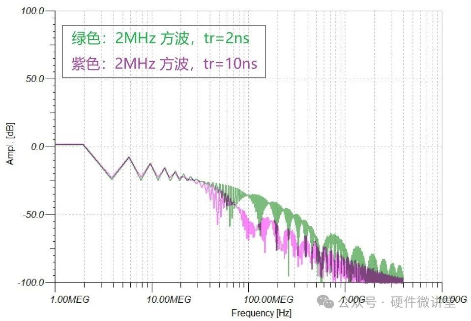
When tr=2ns, f2=159MHz can be roughly calculated. That is, when the frequency is greater than 159MHz, the amplitude of the frequency component decreases at a rate of-40 dB/dec..
When tr=10ns, f2=31.8MHz can be roughly calculated. That is, when the frequency is greater than 31.8MHz, the amplitude of the frequency component begins to decrease at a rate of-40 dB/dec..
From the above picture, we can really see this trend. When the rising edge increases from 2ns to 10ns, the frequency point at which the frequency spectrum decreases at the rate of -40dB/dec is obviously advanced (from 159MHz to 31.8MHz).
Combined with circuit analysis
In front of us, we spent a lot of space to analyze the frequency spectrum of the excitation source, and quantitatively analyzed the envelope asymptote, which is only the analysis of the circuit excitation source. Let's look at the circuit again.
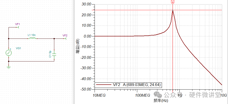
The frequency gain curve of LC circuit, as shown in the above figure, is believed to be familiar to all students. The position of the resonance point is around 689MHz. This resonant frequency belongs to the hardware characteristics of the circuit and will not change with the frequency and rising edge of the excitation source. Whether the excitation source tr is 2ns or 10ns, the resonant frequency and Q value of LC circuit are unchanged.
Combined with the conclusion of the last section, we can know that tr increases from 2ns to 10ns, and the frequency point at which the spectrum begins to decay at the rate of -40dB/dec is advanced from 159MHz to 31.8MHz. When the frequency rises to around 689MHz, the frequency spectrum of the excitation source with tr=10ns is attenuated more and the amplitude is lower than that with tr=2ns. Based on the frequency-selective characteristics of LC resonance, the amplitude after frequency-selective amplification will be smaller than that of tr=2ns.
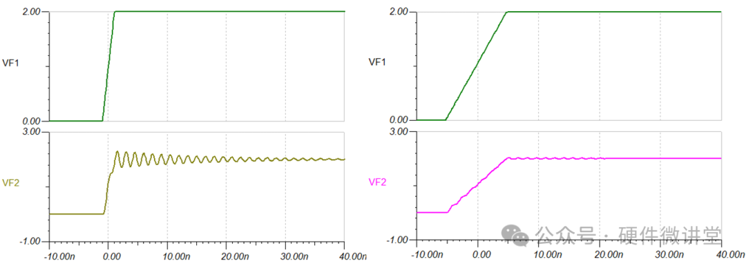
As shown in the above figure, VF1 and VF2 with tr=2ns are on the left, and VF1 and VF2 with tr=10ns are on the right. It can be seen that the ringing at the output is obviously weakened after the tr slows down.
Emphasis: the ringing here is only weakening/inhibiting, not eliminating. Because all the actions mentioned above have not fundamentally changed the working state of the oscillation system, the system is still under-damped. It only weakens the energy of the excitation source entering the oscillation system.
Total knot
Let's stop here and sort out what we discussed today:
① Tell a practical problem: you can't change PCB, circuit parameters and frequency, and you need to suppress ringing. How to break it?
② The spectral envelope and its asymptote of trapezoidal wave are analyzed by the actual simulation waveform;
③ Analyze the spectral envelope difference of trapezoidal wave corresponding to different tr by comparing the actual simulation waveforms;
④ Comparing the ringing suppression of different TRs by combining circuit and simulation;
⑤ The last "emphasized" paragraph tells the essence of the problem, which is particularly important.
About Maxipcb
Maxipcb empowers innovators to turn cutting-edge technologies into reality.
We offer one-stop solutions for design, simulation, testing, PCB manufacturing, component procurement and SMT assembly, enabling efficient development, rapid deployment and risk control across the full product lifecycle.
Serving the world in communications, industrial automation, aerospace, automotive, semiconductor and beyond, we build a safer, more connected future together.


