Static electricity from the human body, the environment, or even inside electronic equipment can cause various types of damage to sensitive semiconductor chips – for example, penetrating thin insulating layers inside components;
Static electricity from the human body, the environment, or even inside electronic equipment can cause various types of damage to sensitive semiconductor chips – for example, penetrating thin insulating layers inside components; destroying the gates of MOSFETs and CMOS devices; latching up flip‑flops in CMOS devices; short‑circuiting reverse‑biased PN junctions; short‑circuiting forward‑biased PN junctions; and melting internal bonding wires or aluminium traces in active devices. To eliminate the interference and damage caused by electrostatic discharge (ESD) to electronic equipment, multiple technical measures must be employed.
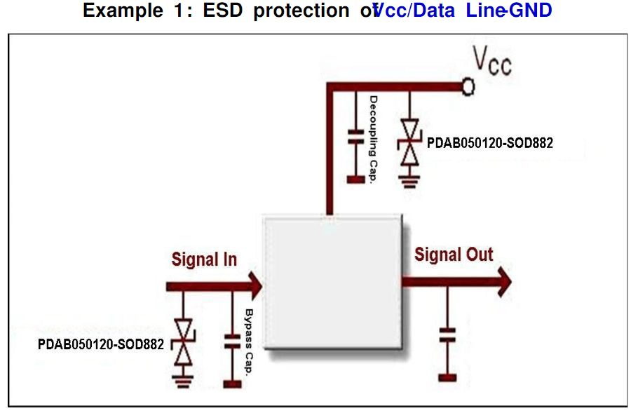
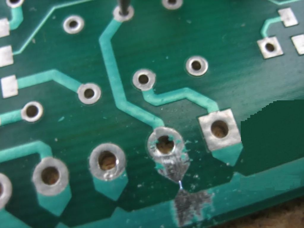
In PCB design, ESD‑hardened designs can be achieved through proper layer stackup, appropriate component placement and routing, and mechanical assembly. During the design process, through prediction, most design modifications can be limited to adding or removing components. By adjusting PCB layout and routing, ESD can be effectively mitigated. The following are some common protective measures.
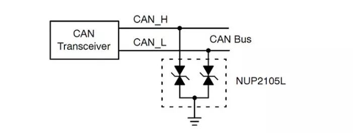
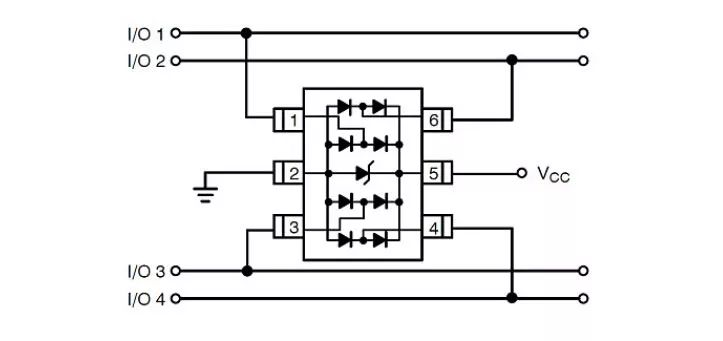
Several Typical General‑Purpose ESD Protection Circuits
Personal Sharing: 9 Practical ESD Protection Measures
Recently, I have been conducting ESD testing on electronic products. From the test results across different products, I have found that ESD testing is a very important exercise: if the circuit board is poorly designed, the introduction of static electricity can cause the product to crash or even damage components. Previously, I only knew that ESD could damage components, but I did not realise how much attention it deserves for electronic products as a whole.
ESD stands for Electro‑Static Discharge. From what we have learned, static electricity is a natural phenomenon, typically generated through contact, friction, or induction between electrical devices. Its characteristics include long‑term accumulation, high voltage (capable of generating several thousand to even tens of thousands of volts), low charge, small current, and short duration. For electronic products, if ESD design is not properly implemented, it often leads to unstable operation or even damage.
Two common methods are used in ESD discharge testing: contact discharge and air discharge.
Contact discharge means discharging directly to the device under test. Air discharge, also known as indirect discharge, is coupling via a strong magnetic field to adjacent current loops. The typical test voltages for these two methods range from 2 kV to 8 kV, with variations depending on regional requirements. Therefore, before starting the design, it is essential to understand the target market for the product.
The above two scenarios are fundamental tests conducted to address situations where electronic products malfunction when touched by humans, due to static charges on the human body or other causes.
Humidity levels vary around the world. Even within the same region, different humidity levels produce different amounts of static electricity. From collected data, it can be seen that static electricity increases as humidity decreases. This indirectly explains why, in northern winters, removing a sweater can generate such large static sparks.
"Given the significant hazards of static electricity, how do we protect against it?" In ESD protection design, we typically follow a three‑step approach: prevent external charges from flowing into the circuit board and causing damage; prevent external magnetic fields from damaging the circuit board; and prevent damage from electrostatic fields.
In actual circuit design, we often use one or more of the following methods for ESD protection:
1. Avalanche Diodes for ESD Protection
This is a commonly used method in design. The typical approach is to connect an avalanche diode from the critical signal line to ground in parallel. This method takes advantage of the fast response and stable clamping capability of avalanche diodes, allowing the accumulated high voltage to be dissipated in a short time, thereby protecting the circuit board.
2. High‑Voltage Capacitors for Circuit Protection
This method typically places ceramic capacitors with a withstand voltage of at least 1.5 kV at I/O connectors or critical signal locations, with connecting leads kept as short as possible to reduce inductive reactance. If capacitors with low withstand voltage are used, they may be damaged and lose their protective function.
3. Ferrite Beads for Circuit Protection
Ferrite beads can effectively attenuate ESD currents and also suppress radiation. When facing both issues, a ferrite bead can be a very good choice.
4. Spark Gap Method
I came across this method in some reference material. The specific implementation involves using triangular copper shapes pointing at each other on a microstrip layer. One triangle is connected to the signal line, and the other to ground. When static electricity occurs, spark discharge occurs at the tip, dissipating the electrical energy.
5. LC Filters for Circuit Protection
LC filters can effectively reduce high‑frequency static electricity entering the circuit. The inductive reactance of the inductor effectively suppresses high‑frequency ESD from entering the circuit, while the capacitor shunts high‑frequency ESD energy to ground. Additionally, this type of filter can smooth signal edges and reduce RF effects, further improving signal integrity.
6. Multilayer Boards for ESD Protection
When budget allows, choosing a multilayer board is also an effective means of ESD protection. In a multilayer board, the presence of a solid ground plane close to the traces allows ESD to couple more quickly to the low‑impedance plane, thereby protecting critical signals.
7. Guard Ring / Protective Band Around the Board
This method typically involves drawing traces around the circuit board without solder mask. Where conditions permit, connect these traces to the chassis. However, care must be taken to ensure that these traces do not form a closed loop, which could act as a loop antenna and introduce further problems.
8. CMOS or TTL Devices with Clamping Diodes for Circuit Protection
This method uses the principle of isolation for circuit protection. Because these devices already have clamping diodes built in, they reduce design complexity in actual circuit design.
9. Extensive Use of Decoupling Capacitors
These decoupling capacitors should have low ESL and ESR values. For low‑frequency ESD, decoupling capacitors reduce the loop area, and due to their ESL, the dielectric effect is weakened, allowing better filtering of high‑frequency energy.
In summary, although ESD is formidable and can have serious consequences, as long as the power and signal lines on the circuit are well protected, ESD currents can be effectively prevented from entering the PCB. As my boss often says, "A good grounding scheme is the key to a good board." I hope this insight can also be enlightening for everyone.
Additional ESD Protection Details
-
Use multilayer PCBs whenever possible. Compared with double‑side boards, ground planes and power planes, together with closely spaced signal‑to‑ground trace spacing, reduce common‑mode impedance and inductive coupling to 1/10 to 1/100 of that of double‑side boards. Place each signal layer as close as possible to a power or ground layer. For high‑density boards with components on both the top and bottom surfaces, short connecting traces, and extensive ground fills, consider using inner‑layer routing.
-
For double‑side PCBs, use a tightly interwoven power and ground grid. Place power and ground traces close together, with as many connections as possible between vertical and horizontal lines or fill areas. The grid spacing on one side should be ≤ 60 mm; if possible, reduce it to ≤ 13 mm.
-
Ensure that every circuit is as compact as possible.
-
Place all connectors on one side of the board if possible.
-
If possible, bring the power supply into the card from the centre, away from areas that are directly susceptible to ESD.
-
On all PCB layers beneath connectors that lead to the outside of the chassis (and are therefore directly exposed to ESD), place wide chassis‑ground traces or polygon‑filled ground areas, and connect them together with vias at intervals of approximately 13 mm.
-
Place mounting holes at the edges of the board, with top‑ and bottom‑layer pads (without solder mask) around them connected to chassis ground.
-
During PCB assembly, do not apply any solder to the top‑ or bottom‑layer pads. Use screws with built‑in washers to achieve firm contact between the PCB and the metal chassis/shield or mounting bracket.
-
Provide the same "isolation gap" between chassis ground and circuit ground on each layer. If possible, maintain a spacing of 0.64 mm.
-
On the top and bottom layers, near the mounting holes, connect chassis ground to circuit ground with 1.27‑mm‑wide traces at intervals of 100 mm along the chassis‑ground line. Adjacent to these connection points, place mounting pads or holes between chassis ground and circuit ground. These ground connections can be opened with a blade to keep them open, or bridged with a ferrite bead or high‑frequency capacitor.
-
If the board will not be placed in a metal chassis or shielding enclosure, do not apply solder mask to the chassis‑ground traces on the top and bottom layers, so that they can serve as discharge electrodes for ESD arcing.
-
Create a guard ring around the circuit in the following manner:
(1) Place a guard‑ring trace around the entire perimeter, except for edge connectors and chassis ground.
(2) Ensure that the guard‑ring width on all layers is greater than 2.5 mm.
(3) Connect the guard ring with vias at intervals of 13 mm.
(4) Connect the guard ring to the common circuit ground of the multilayer board.
(5) For double‑side boards mounted in a metal chassis or shielding enclosure, connect the guard ring to the circuit common ground. For unshielded double‑side boards, connect the guard ring to chassis ground. Do not apply solder mask on the guard ring so that it can act as an ESD discharge rod. Leave at least one 0.5‑mm‑wide gap at some point on the guard ring (on all layers) to avoid forming a large loop. Keep signal traces at least 0.5 mm away from the guard ring.
-
Route a ground trace adjacent to every signal line in areas directly susceptible to ESD strikes.
-
Place I/O circuits as close as possible to their corresponding connectors.
-
Place ESD‑sensitive circuits near the centre of the board, where other circuits can provide some shielding.
-
Place series resistors or ferrite beads at the receiver end; for cable drivers that are susceptible to ESD, consider placing series resistors or ferrite beads at the driver end as well.
-
Place transient suppressors at the receiver end. Connect them to chassis ground with short, wide traces (length < 5 times width, preferably < 3 times width). Signal and ground lines from the connector should go directly to the transient suppressor before connecting to the rest of the circuit.
-
Place filter capacitors at the connector or within 25 mm of the receiver circuit.
(1) Connect them to chassis ground or receiver circuit ground with short, wide traces (length < 5 times width, preferably < 3 times width).
(2) Connect signal and ground lines to the capacitor first, then to the receiver circuit.
-
Ensure that signal traces are as short as possible.
-
When signal trace length exceeds 300 mm, run a ground trace in parallel with it.
-
Minimise the loop area between signal traces and their corresponding return paths. For long signal traces, swap the positions of the signal and ground traces every few centimetres to reduce loop area.
-
Drive signals from the centre of the network to multiple receiver circuits.
-
Minimise the loop area between power and ground. Place a high‑frequency capacitor near every power pin of each IC.
-
Place a high‑frequency bypass capacitor within 80 mm of each connector.
-
Fill unused areas with ground copper wherever possible, and connect the ground fills on all layers together at intervals of 60 mm.
-
Ensure that any large ground‑fill area (approximately > 25 mm × 6 mm) is connected to ground at two opposite points.
-
When an opening in a power or ground plane exceeds 8 mm in length, connect the two sides of the opening with a narrow trace.
-
Do not route reset lines, interrupt signals, or edge‑triggered signals near the edge of the PCB.
-
Connect mounting holes to circuit common ground or isolate them.
(1) When metal brackets must be used together with metal shielding or chassis, use a 0 Ω resistor to make the connection.
(2) Determine the mounting‑hole size to allow reliable installation of metal or plastic brackets. Use large pads on the top and bottom layers of the mounting holes; do not apply solder mask to the bottom‑layer pads, and ensure that the bottom‑layer pads are not wave‑soldered.
-
Do not route protected and unprotected signal lines in parallel.
-
Pay special attention to the routing of reset, interrupt, and control signal lines:
(1) Use high‑frequency filtering.
(2) Keep them away from input and output circuits.
(3) Keep them away from the board edges.
-
Insert the PCB into the chassis – do not mount it at openings or internal seams.
-
Pay attention to routing under ferrite beads, between pads, and near signal lines that may come into contact with ferrite beads. Some ferrite beads are quite conductive and may create unintended conduction paths.
-
If a chassis or motherboard contains multiple PCBs, place the most ESD‑sensitive board in the middle.
About Maxipcb
Maxipcb empowers innovators to turn cutting-edge technologies into reality.We offer one-stop solutions for design, simulation, testing, PCB manufacturing, component procurement and SMT assembly, enabling efficient development, rapid deployment and risk control across the full product lifecycle.
Serving the world in communications, industrial automation, aerospace, automotive, semiconductor and beyond, we build a safer, more connected future together.

