The packaging process is the last process of semiconductor manufacturing, and its sequence is grinding, cutting, pasting, wire bonding and molding. The sequence of these processes can be changed according to the change of packaging technology, and can also be closely related or merged with each other.
The packaging process is the last process of semiconductor manufacturing, and its sequence is grinding, cutting, pasting, wire bonding and molding. The sequence of these processes can be changed according to the change of packaging technology, and can also be closely related or merged with each other. This paper mainly introduces wafer bonding, which is a packaging technology, and is used to bond the chip separated from the wafer with the packaging substrate (lead frame or PCB) after the dicing process.
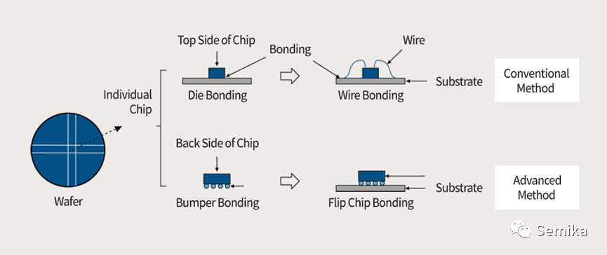
Figure 1, Types of Bonding
In semiconductor technology, "bonding" refers to connecting a wafer chip to a substrate. Bonding can be divided into two types, namely traditional methods and advanced methods. Traditional methods include chip connection (or chip connection) and wire connection, while advanced methods include flip-chip connection developed by IBM in the late 1960s. Flip-chip bonding is a method combining die bonding and wire bonding, which is a method of connecting the chip and the substrate by forming bumps on the chip pad.
Just as an engine is installed in an automobile to provide power, a semiconductor chip is bonded to a lead frame or a printed circuit board (PCB) to connect the chip with the outside. After the chip is bonded, it should be able to withstand the physical pressure generated after packaging and radiate the heat generated when the chip works. When necessary, it must maintain constant conductivity or achieve a high level of insulation. Therefore, as the chip becomes smaller and smaller, the bonding method becomes more and more important.
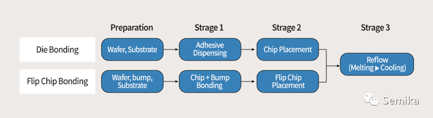
Figure 2. Comparison between Chip Bonding and Flip Chip Bonding
For chip bonding, the first thing to do is to coat adhesive on the package substrate. Then, put a chip on it with the pins facing up. On the contrary, in the case of flip-chip bonding, this is a more advanced method, and small bumps called solder balls are attached to the pads of the chip. Then, place the chip on the substrate with the pins facing down. In these two methods, the assembled unit passes through a temperature reflux channel, which can adjust the temperature over time to melt the adhesive or solder balls. Then, it is cooled to fix the chip (or bump) on the substrate.
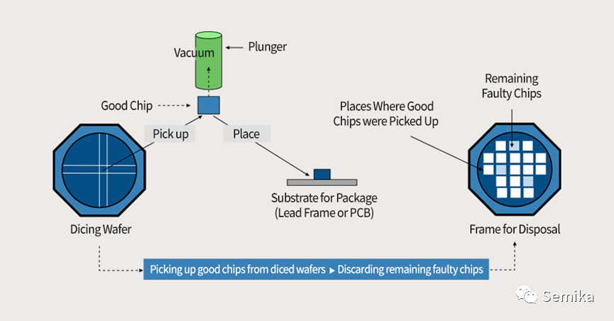
Figure 3. Chip Picking and Placement
It is called "Pick" to take out the chips attached to the tape separately. When the good chips are taken out from the wafer by the plunger, placing them on the surface of the package substrate is called "Place". These two tasks, called "Pick & Place", were completed on a Die Bonde. After the chip is bonded, the bad pieces that have not been removed remain on the tape and are all discarded when the frame is recycled. In this process, the good chips are sorted by inputting the wafer test results (Go/No Go) in Mapping Table2.
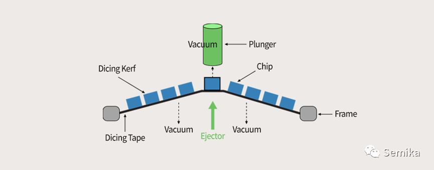
Fig. 4. Chip ejection: an enlarged view of the force applied in three directions.
Each chip should be separated separately and adhered to the dicing tape with weak adhesion. At this time, it is not so easy to pick up the chips placed horizontally on the tape one by one. This is because it is not easy to fall off even if it is pulled up by a vacuum extractor. If it is forcibly pulled out, it will cause physical damage to the chip.
Therefore, an easy way to pick up the chip is used: "ejection". The ejector is used to exert physical force on the target chip, which makes it slightly different from other chips. After the chip is ejected from the bottom, use a vacuum belt plunger to pull the chip from above. At the same time, pull the bottom of the tape with vacuum to make the tape surface smooth. When bonding chips, connection by using solder or paste containing metal (Power Tr), or polymer (polyimide) can also be used for chip bonding. In polymer materials, silver-containing paste or liquid epoxy resin is relatively easy to use and has a high frequency of use.
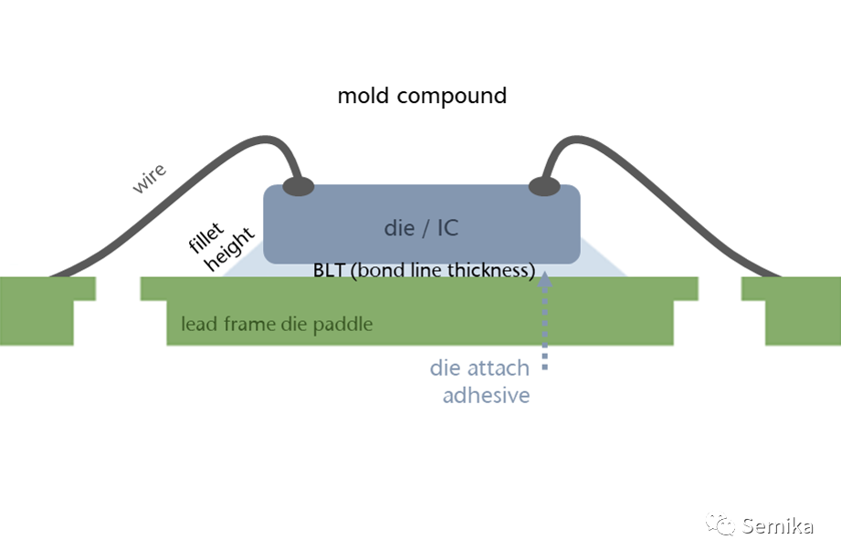
When epoxy resin is used for chip bonding, a very small amount of epoxy resin is accurately coated on the substrate by dispensing. After placing the chip on it, the epoxy resin is hardened at 150 to 250°C by reflow or curing, so as to bond the chip and the substrate together. At this time, if the thickness of the coated epoxy resin is not constant, warping may occur due to the difference in thermal expansion coefficient. For this reason, although it is more advantageous when the amount of epoxy resin is small, any form of warping will occur as long as epoxy resin is used.
This is why a more advanced bonding method, die attach film (DAF), has been used recently. Although DAF has some disadvantages of being expensive and difficult to handle, it is easy to apply a certain amount, which simplifies the process, so its usage is increasing gradually.
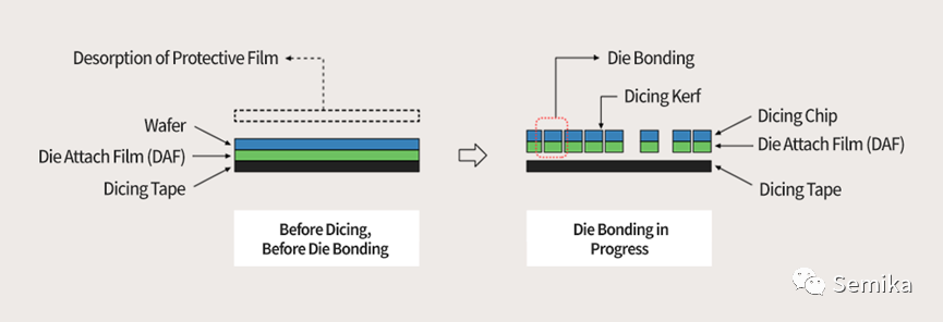
Figure 6. Die Bonding with Die Bonding Film (DAF)
DAF is a thin film attached to the bottom of a chip. The thickness of DAF can be adjusted to a very thin and constant thickness. It is widely used not only in the bonding between chips and substrates, but also in the bonding between chips to create a multi-chip package (MCP). From the structure of the chip, the DAF at the bottom of the chip is stuck to the chip, while the dicing tape is stuck to the DAF below it, with weak adhesion. For chip bonding in this structure, after the chip and DAF are removed from the adhesive tape, the chip is directly placed on the substrate without using epoxy resin. Because the dispensing process can be skipped in this process, the disadvantages of epoxy resin are not brought in, but the performance of DAF.
When using DAF, some air can penetrate the film, causing problems such as film deformation. In particular, the equipment for handling DAF requires high precision. However, the use of DAF is the main reason, because it can reduce the defect rate and improve the productivity, because it simplifies the process and increases the thickness uniformity.
Depending on the type of substrate (lead frame or PCB), the direction of chip bonding varies greatly. For a long time, pcb-based substrates have been frequently used because it can mass-produce small-sized packages. Therefore, with the diversification of bonding technology, the temperature distribution of baking adhesive is also developing. Typical bonding methods are thermal compression or ultrasonic bonding. With the development of ultra-thin packaging, the degree of integration is constantly improving, and the packaging technology is also diversified.
About Maxipcb
Maxipcb empowers innovators to turn cutting-edge technologies into reality.
We offer one-stop solutions for design, simulation, testing, PCB manufacturing, component procurement and SMT assembly, enabling efficient development, rapid deployment and risk control across the full product lifecycle.Serving the world in communications, industrial automation, aerospace, automotive, semiconductor and beyond, we build a safer, more connected future together. 


