In recent years, in order to meet the needs of miniaturization of some high-end consumer electronic products, the integration of chips is getting higher and higher, the pitch of BGA pins is getting closer and closer (less than or equal to 0.4pitch), the layout of PCB is becoming more and more compact, and the wiring density is getting larger and larger. In order to improve the routing rate of the design without affecting the performance such as signal integrity, ANYLAYER technology is applied.
ANYLAYER technologyIn recent years, in order to meet the needs of miniaturization of some high-end consumer electronic products, the integration of chips is getting higher and higher, the pitch of BGA pins is getting closer and closer (less than or equal to 0.4pitch), the layout of PCB is becoming more and more compact, and the wiring density is getting larger and larger. In order to improve the routing rate of the design without affecting the performance such as signal integrity, ANYLAYER technology is applied. This is the Alivh-any layer IVH structure multilayer printed wiring board.
Technical characteristics of arbitrary layer viasCompared with HDI technology, the biggest advantage of ALIVH is that the design freedom is greatly increased, and holes can be punched at will between layers, which HDI technology cannot do. Generally, the most complicated structure of domestic manufacturers, that is, the design limit of HDI is the third-order HDI board. Because HDI does not completely use laser drilling, the buried holes in the inner layer use mechanical holes, so the requirements of the hole plate are much larger than those of the laser holes, and the mechanical holes occupy the space on the passing plane. Therefore, generally speaking, compared with the arbitrary drilling of ALIVH technology, the aperture of the inner core plate can also be 0.2mm micropores, which is still a big gap. Therefore, the routing space of ALIVH board is probably much better than that of HDI. At the same time, the cost and processing difficulty of ALIVH are higher than that of HDI process. As shown in figure 3, it is a schematic diagram of ALIVH.
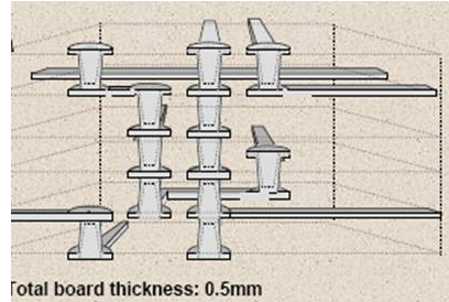
Fig. 3 schematic diagram of ALIVH
Design challenges of vias with arbitrary layersAny layer via technology completely subverts the traditional via design method. If you still need to set different layers of vias, it will increase the management difficulty. It is necessary to design tools with the ability of intelligent punching, and at the same time, they can be combined and split at will.
In addition to the traditional wiring method based on line changing layer, Cadence adds the line changing method based on Working Layer, as shown in Figure 4: You can check the layer that can be looped in the Working Layer panel, and then when you double-click to punch holes, you can select any layer to change lines.
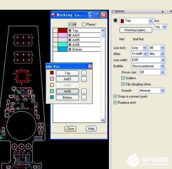
Figure 4 Wiring Mode Based on Working Layer
Example of ALIVH design and board making:10-story ELIC design
OMAP™ 4 Platform
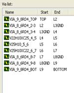
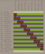
Figure 5 ALIVH design board case
Buried resistance, buried capacity and embedded componentsHigh-speed access to the Internet and social networks requires high integration and miniaturization of handheld devices. At present, it relies on the most advanced 4-N-4 HDI technology. But for the next generation of new technology and higher interconnection density, in this field, embedding passive or even active parts into PCB and substrate can meet the above requirements. When you design consumer electronic products such as mobile phones and digital cameras, it is the best choice to consider how to bury passive and active parts in PCB and substrate. This method may be slightly different because you use different suppliers. Another advantage of embedded parts is that the technology provides protection for intellectual property rights and prevents so-called reverse design. Allegro PCB Editor can provide the best industrial-grade solution. Allegro PCB Editor can also work more closely with HDI boards, flexible boards and embedded parts. You can get the correct parameters and constraints to complete the design of embedded parts. The design of embedded devices can not only simplify the SMT process, but also greatly improve the cleanliness of products.
Buried resistance and capacity designBuried resistance, also known as buried resistance or thin film resistance, is to press a special resistance material on an insulating substrate, and then obtain the required resistance value through printing, etching and other processes, and then press it together with other PCB layers to form a planar resistance layer. The common manufacturing technology of PTFE buried resistance multilayer printed board can achieve the required resistance accuracy.
Buried capacitance is to use materials with high capacitance density and reduce the distance between layers to form a large enough capacitance between plates to decouple and filter the power supply system, thus reducing the discrete capacitance required on the plate and achieving better high-frequency filtering characteristics. Because the parasitic inductance of buried capacitor is very small, its resonance frequency point will be better than that of ordinary capacitor or low ESL capacitor.
Due to the maturity of technology and technology, and the need of high-speed design for power supply system, the technology of buried capacitance is applied more and more. To use buried capacitance technology, we must first calculate the size of plate capacitance, and the formula is as follows:
C =

Fig. 6 Calculation formula of plate capacitance
Among them:
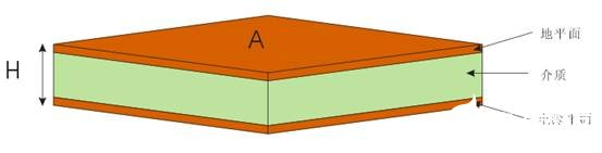
C is the capacitance of buried capacitance (plate capacitance)
A is the area of flat plates, and it is difficult to increase the area between flat plates when the structure of most designs is determined.
D_k is the dielectric constant of the medium between plates, and the capacitance between plates is directly proportional to the dielectric constant.
K is Vacuum permittivity, also known as vacuum permittivity, which is a physical constant with a value of 8.854 187 818× 10-12 farad/meter (f/m).
H is the thickness between planes, and the capacitance between plates is inversely proportional to the thickness, so we need to reduce the interlayer thickness if we want to get a larger capacitance. The interlayer dielectric thickness of 3M C-ply buried material can reach 0.56mil, and the dielectric constant of 16 greatly increases the capacitance between plates.
Through calculation, 3M C-ply buried material can achieve 6.42nF capacitance between plates per square inch.
At the same time, it is necessary to use PI simulation tool to simulate the target impedance of PDN, so as to determine the capacitor design scheme of single board and avoid the redundant design of buried capacitor and discrete capacitor. Fig. 7 is the PI simulation result of a buried capacitance design, which only considers the effect of inter-board capacitance and does not add the effect of discrete capacitance. It can be seen that only by increasing the buried capacity, the performance of the whole power supply impedance curve is greatly improved, especially above 500MHZ, which is a frequency band where the board-level discrete filter capacitor is difficult to work, and the plate capacitor can effectively reduce the power supply impedance.
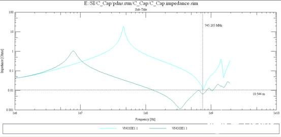
Fig. 7 Effect of Buried Capacity on PI
Buried capacity design case:28-story board and 4-story buried capacity design
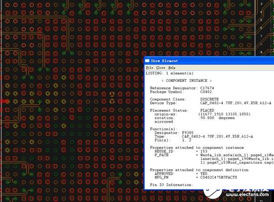
Figure 8 Case of Buried Capacity Design
About MaxipcbMaxipcb inspires and empowers innovators and helps them bring world-changing technologies to life. We provide advanced design, simulation and testing solutions to help engineers complete development and deployment faster in the whole product life cycle, while controlling risks. Our customers are all over the world, such as communication, industrial automation, aerospace and national defense, automobile, semiconductor and general electronics. We join hands with customers to accelerate innovation and create a safe and interconnected world.


