With the development of high-speed serial bus technology, the signal transmission rate continues to increase, and the influence of parasitic parameters of vias has been paid more and more attention. High-speed simulation engineers pay attention to the optimization of vias and reduce the influence of parasitic parameters of vias by various means. HDI can reduce the parasitic parameters of surface devices due to the design requirements of holes in the disk.
With the development of high-speed serial bus technology, the signal transmission rate continues to increase, and the influence of parasitic parameters of vias has been paid more and more attention. High-speed simulation engineers pay attention to the optimization of vias and reduce the influence of parasitic parameters of vias by various means. HDI can reduce the parasitic parameters of surface devices due to the design requirements of holes in the disk. At the same time, the inductance and capacitance of micropores are only about one tenth of that of a standard via. Figure 9 shows the via inductance and capacitance that can be found in many materials, which are obtained according to the following two calculation formulas.
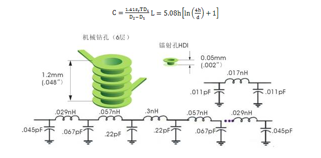
Fig. 9 Parasitic parameters of laser holes and mechanical holes However, there are still many problems in fig. 7. The parasitic capacitance is the capacitance to the ground, and all six layers of mechanical holes will not be connected to the ground plane, so the calculation will be far more complicated than the formula. At present, when vias are produced, the diskless process is basically adopted, that is, the via pads of non-connected layers are removed, which can effectively reduce the parasitic capacitance of vias. In this case, it is not enough to simply consider the influence of via characteristic impedance only by the realization and application of miniaturization design -3.
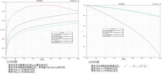
Fig. 10 is an analysis of insertion loss and return loss of micropores and common mechanical holes from S parameters.
Realization and Application of Miniaturization Design -3
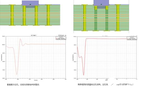
Figure X Analysis of Insertion Loss of Micro-holes and Ordinary Mechanical Holes by S Parameter
Then through the TDR formula, we can see that the impedance of the via hole is closely related to the return loss curve. The simulation accuracy of S11 in the whole frequency band also determines the accuracy of studying the impedance by looking at the TDR curve through software simulation, as shown in Figure 11:
TDRZ(t) = Zref*(1+IFFT(S11*input)) / (1-IFFT(S11*input))
It can be seen that backdrilling still has a great influence on the via impedance.
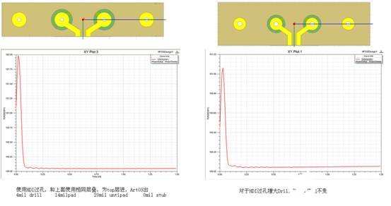
The impedance of differential HDI micropores is close to 100 ohms.
Figure 11 Optimization strategy of differential vias and TDR simulation results.
The impedance of micro-holes can be easily optimized to the impedance value of 100 ohms of differential lines, thus reducing the high-speed problem caused by impedance discontinuity caused by vias.
From the above analysis, it can be seen that the high-speed performance of micro-holes is far superior to that of ordinary mechanical holes, and there is no problem of Stub. Even if the back drilling process is adopted for mechanical holes, a certain length of Stub will inevitably appear. And this Stub is often a fatal killer that affects the performance of high-speed circuits.
If you are concerned about the overcurrent capacity of micropores, copper can be filled in micropores to improve the current carrying capacity when necessary.
Conclusion
Cadence's SPB16.X platform provides excellent miniaturization design capability, and provides excellent support in HDI multi-level via design, arbitrary-level via design, embedded device design and embedded capacity simulation analysis based on PDN. The constraint manager, which is optimized and updated based on HDI, helps engineers to realize constraint-driven layout in the field of miniaturization design, improve design efficiency and ensure design success rate.
Based on Cadence's powerful platform and rich experience in HDI design, combined with the leading HDI processing capabilities of its own board factory and partners in China, MaxiPCB can provide all-round one-stop services such as miniaturization design, simulation, production, mounting and assembly, and fully realize the various needs of customers in the miniaturization field.
MaxiPCB and Cadence cooperated to launch the book Cadence printed circuit board design-Allegro PCB Editor design guide, which also introduces the miniaturization design technology. Welcome to consult and exchange.
references
[1] cadence printed circuit board design-Allegro PCB Editor design guide.
[2] 《High-Speed Digital Design – A Handbook of Black Magic》
Thank you!
This paper quotes the miniaturization chapter of Cadence PCB Design-Allegro PCB Editor, which Wang Hui is responsible for. At the same time, the simulation part has done a lot of communication with Cadence Zhong Zhangming. Thank you!
About MaxipcbMaxipcb inspires and empowers innovators and helps them bring world-changing technologies to life. We provide advanced design, simulation and testing solutions to help engineers complete development and deployment faster in the whole product life cycle, while controlling risks. Our customers are all over the world, such as communication, industrial automation, aerospace and national defense, automobile, semiconductor and general electronics. We join hands with customers to accelerate innovation and create a safe and interconnected world. 


