A control product failed RE (Radiated Emission) and CE (Conducted Emission) tests due to serious defects in PCB layout and routing.
1. EMC Failure Case 1 – Control Product
A control product failed RE (Radiated Emission) and CE (Conducted Emission) tests due to serious defects in PCB layout and routing.
PCB Design Issues
-
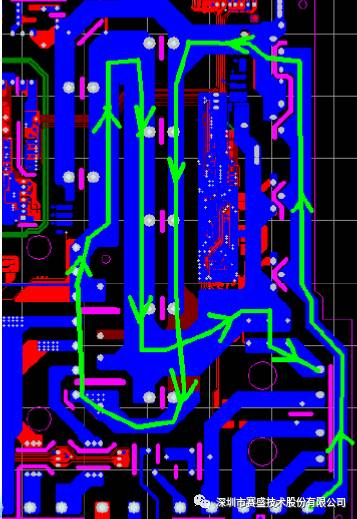
DC power input traces are tortuous, creating large loops that easily cause spatial coupling and reduce filtering performance.
-
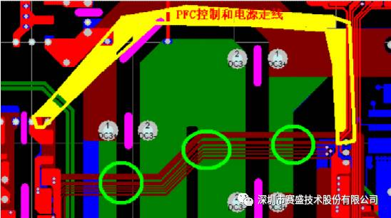
PFC power traces run together with control signal lines.
PFC is a strong noise source, leading to serious interference on control signals.
-
Some signal traces run too close to the PCB edge without ground protection, causing excessive outward radiation.
PCB Design Recommendations
-
Optimize layout to follow
current flow direction. Route positive and negative power lines in parallel to minimize loop area.
-
Reroute control signals away from PFC power lines to prevent noise radiation.
-
Apply guard grounding to signals, add ground copper at board edges, and separate different signal types with ground traces to suppress crosstalk.
2. EMC Failure Case 2 – Electronic Learning Machine (LCD Module)
An electronic learning machine with an LCD failed radiation testing. The main noise source was the
LCD board and flat cable.
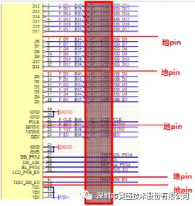
Problems
- Insufficient ground pins at the LCD interface, resulting in long return paths and strong radiated emissions.
- The PCB is a 2-layer board for LCD power and signals.
Improvement Suggestions
- Add more ground pins to the LCD interface to shorten return paths.
- No need to split analog and digital ground; merge grounds or connect with a 0Ω resistor.
- Move Vcc power trace below the connector to avoid coupling noise onto the flat cable.
- Relocate long signal traces downward to avoid crossing ground splits.
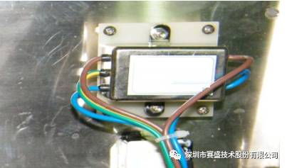
3. Structural Design Review – Instrument Power Interface
The design intended to add a filter to the AC power port to reduce EMI and improve EMS immunity.
However,
input and output cables were bundled together, allowing noise to bypass the filter via capacitive coupling, making the filter ineffective.
Recommendation
Do not bundle input and output cables. Route them
180° opposite to minimize coupling.
 About Maxipcb
Maxipcb empowers innovators to turn cutting-edge technologies into reality.
We offer one-stop solutions for design, simulation, testing, PCB manufacturing, component procurement and SMT assembly, enabling efficient development, rapid deployment and risk control across the full product lifecycle.Serving the world in communications, industrial automation, aerospace, automotive, semiconductor and beyond, we build a safer, more connected future together.


