In today's industry, there are two main mainstream assembly technologies:
1. Surface mount technologyFor some extremely small and sensitive components, such as resistors or diodes, they will be placed on the surface of the circuit board in an automatic way. Electronic components mounted in this way are called surface mount devices (SMD). Refer to Figure 2 for details.
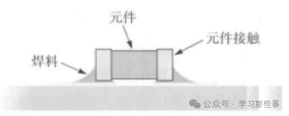
Figure 2: Surface Mount Technology
2. Through hole technologyThis technology is suitable for those components with leads or wires. Such components need to be inserted into holes on the board to be mounted on the circuit board. After insertion, the redundant lead parts need to be soldered on the other side of the circuit board, as shown in Figure 3. Through-hole technology is often used in the assembly of printed circuit boards including capacitors, coils and other large components.
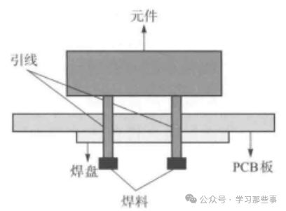
Figure 3: Through-hole technology
Actual PCB assembly process steps1. Solder paste templateThe first step in the assembly process of printed circuit board is to apply solder paste on the circuit board. This process is similar to screen printing of shirts, but the difference is that the printed circuit board is not an ordinary mask, but a thin stainless steel template. With the help of this template, the assembler can accurately apply solder paste only on specific expected parts of the printed circuit board. These parts are exactly where the components on the finished printed circuit board are to be placed. The solder paste itself appears as a gray substance, which is composed of tiny metal balls, which are commonly called solder. Its composition contains 96.5% tin, 3% silver and 0.5% copper. Solder paste mixes solder and flux together. As a chemical substance, flux can help solder melt and make it better adhere to the surface of circuit board. The solder paste that appears gray must be applied to the correct position of the circuit board in a precise amount. In the professional PCB assembly process production line, the mechanical fixture will firmly fix the PCB and the welding template, and the daubing device will accurately place the appropriate amount of solder paste in the expected area. Subsequently, the machine will evenly spread the paste solder paste on the template and ensure that each open area can be evenly covered. After the template is removed, the solder paste will remain in the predetermined position.
2. Pick and place operationAfter the PCB was successfully coated with solder paste, the PCB assembly process line was transferred to the mounter. At this time, the automatic mechanical equipment will place surface mount components, that is, surface mount devices (SMD), on the prepared printed circuit board. SMD occupies a considerable proportion in the current non-connector components of printed circuit boards. Subsequently, in the next step of the PCB assembly process, these SMDs will be soldered to the surface of the PCB. In the traditional process, this link needs a pair of tweezers, and the assembler manually completes the operation of picking and placing components. Nowadays, the automatic robot arm has replaced manual operation, which is not only more accurate, but also far more consistent than manual operation. In the process of picking and placing, the equipment will use vacuum fixture to pick up the printed circuit board and move it to the picking and placing station. Then, the robot arm will accurately position the printed circuit board on the workstation, and then begin to apply surface mount technology (SMT) to the surface of the printed circuit board. These components will be placed on top of the solder paste in the pre-programmed position.
3. Reflow weldingWhen the solder paste and surface mount components are all in place, it is necessary to ensure that they are firmly attached to the circuit board. This means that the solder paste should be cured, so that the components can be firmly adhered to the circuit board. PCB assembly achieves this goal through a process called "reflow". After the pick-and-place process, the printed circuit board will be transferred to the conveyor belt. This conveyor belt will pass through a large reflux furnace. The reflow oven is similar to a large oven and consists of a series of heaters, which will gradually heat the circuit board to about 250℃, which is enough to melt the solder in the solder paste.
When the solder melts, the printed circuit board will continue to move in the reflow oven and pass through a series of coolers and heaters, so that the melted solder can be cooled and solidified in a controlled way. In this way, a permanent solder joint will be formed to successfully connect SMD with printed circuit board. For many PCB assembly processes, especially the double-sided PCB assembly, special treatment is needed in the reflow process. The assembly of double-sided printed circuit board needs template printing and reflow operation on each side respectively. First, stencil printing, component placement and reflow processing are carried out on the side with fewer parts and smaller size, and then the same operation is carried out on the other side.
4. Inspection and quality controlSurface mount components are soldered in place after reflow process, which does not mean that the assembly process of printed circuit board is completed. The assembled circuit board needs to be tested for function. Usually, the movement in the reflow process may lead to poor connection quality, or even an open circuit with no connection at all. When the component is placed in the wrong position, sometimes it will connect the circuit parts that should not be connected originally, thus causing a short circuit.
Several different inspection methods may be used to check these errors and misalignments. The most common inspection methods include:
1) Manual inspection: Although the development trend of automation and intelligent manufacturing is increasingly obvious, manual inspection is still necessary in the assembly process of printed circuit boards. For small batch production, visual inspection by designers is an effective means to ensure the quality of printed circuit boards after reflow process. However, with the increase of the number of circuit boards to be inspected, this method gradually becomes unrealistic and its accuracy decreases. Observing such a tiny component for a long time will easily lead to visual fatigue, which will lead to inaccurate inspection results.
2) Automatic optical inspection: Automatic optical inspection is a more suitable inspection method for large-scale PCB assembly process. Automated optical inspection (AOI) uses a series of high-power cameras to "view" printed circuit boards. These cameras are arranged at different angles to observe the welding connection. Different quality solder connections reflect light in different ways, which enables AOI to identify lower quality solder. AOI can perform this operation at a very high speed, so it can handle a large number of printed circuit boards in a relatively short time.
3)X-ray inspection: Another inspection method involves X-rays. This is a relatively uncommon inspection method, which is mainly applied to more complex or layered printed circuit boards. X-ray can let the observer penetrate all layers of the circuit board and visualize the lower layers, thus identifying any potential hidden problems.
For the faulty circuit board, it will be sent back for cleaning and rework. If it cannot be repaired, it can only be scrapped. Whether these errors are found during inspection or not, the next step of the process is to test the parts to ensure that they can achieve the expected functions. This involves testing the connection quality of printed circuit boards. For those circuit boards that need to be programmed or calibrated, more steps are needed to test whether their functions are correct. Such inspections can be carried out periodically after the reflow process to identify potential problems. These regular inspections can ensure that errors are found and fixed as soon as possible, which helps manufacturers and designers to save time, manpower and material costs.
5. Insert the through-hole elementDepending on the type of printed circuit board involved in the assembly process of printed circuit board, besides the common surface mount devices (SMD), the circuit board may also contain various components, among which there are plating through hole (PTH) components or through-hole in-line component components. Electroplated through-hole assembly is actually a plated hole on the printed circuit board that runs through the circuit board. The components on the printed circuit board use these holes to realize the transmission of signals on both sides of the circuit board. However, the existence of such components may affect the solder paste, because the solder paste may directly pass through these holes and cannot be effectively adhered to the required position.
PTH components do not use solder paste, but in the subsequent assembly of printed circuit boards, more professional welding methods are needed, such as manual welding or wave soldering. The operation of manually welding the inserted through hole is relatively simple. In general, in a single workstation, a staff member is responsible for inserting a component into the designated PTH hole. After completion, the circuit board will be moved to the next station, and another worker will insert different components. For each PTH hole that needs to be assembled, this cycle is repeated. This process may be time-consuming, depending on the number of PTH components to be inserted in one cycle of PCB assembly process. In view of this, most companies try to avoid using PTH components in their design, but PTH components are still common in actual printed circuit board design. Wave soldering is an automatic form of manual welding, but its operation process is quite different. Once the PTH assembly is in place, the circuit board will be placed on another conveyor belt. This conveyor belt will pass through a special oven. In the oven, a stream of molten solder will wash the bottom of the circuit board and weld all the pins at the bottom of the circuit board at one time. However, this welding method is almost impossible for a double-sided printed circuit board, because a comprehensive welding of one side of the circuit board may damage any precise electronic components on the board. After completing this welding process, the printed circuit board can enter the final inspection link; If additional parts need to be added to the circuit board or the other side needs to be assembled, the previous steps must be repeated.
6. Final inspection and functional testAfter all the soldering steps of the PCB assembly process are completed, the final inspection will be carried out. This inspection aims to test the function of the PCB, which is also called "functional test". This test will simulate the normal environment in which the printed circuit board actually runs, so as to test it. During the test, power and analog signals will pass through the printed circuit board, and at the same time, testers will closely monitor the electrical characteristics of the printed circuit board. Once these characteristics, such as voltage, current or signal output, appear unacceptable fluctuations, or exceed the preset range peak, then the test of the printed circuit board is judged as a failure. For printed circuit boards that fail the test, they can be recycled or scrapped directly according to the specific acceptance criteria. Testing is the last and crucial step in the process of PCB assembly, because it directly determines the success or failure of the whole assembly process. This is why it is so important to test and check regularly during the whole assembly process.
7. Post-cleaning of assembly processIn the process of PCB assembly, a certain amount of flux will remain in the solder paste, and during manual operation, oil stains and dirt on the fingers and clothes of workers may also be transferred to the surface of PCB. After all the assembly work is completed, the surface of the circuit board may appear a little dim, which not only affects the appearance, but also has practical problems.
After several months, the flux left on the printed circuit board began to smell, and became sticky and sour, which would damage the solder joints over time. In addition, when the newly produced printed circuit board is shipped, the surface is covered with residues and fingerprints, and customer satisfaction is often greatly reduced. For the above reasons, it is very important to clean the product after all welding steps are completed. Stainless steel high-pressure cleaning equipment using deionized water is the best tool to remove PCB residues. Cleaning the printed circuit board with deionized water will not pose a threat to the device. This is because ions in ordinary water are the source of damage to the circuit, not the water itself. Therefore, it is safe and harmless to use deionized water to wash the printed circuit board circularly. After cleaning, compressed air is used for rapid circulation drying, so that the finished printed circuit board can be fully prepared for packaging and transportation.
About Maxipcb
Maxipcb empowers innovators to turn cutting-edge technologies into reality.
We offer one-stop solutions for design, simulation, testing, PCB manufacturing, component procurement and SMT assembly, enabling efficient development, rapid deployment and risk control across the full product lifecycle.
Serving the world in communications, industrial automation, aerospace, automotive, semiconductor and beyond, we build a safer, more connected future together.


