"Explore the popular trends in PCB circuit board design."
In the early 1980s, a typical PCB in an 8-bit home computer looked like this:
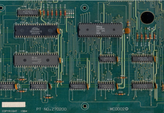
Details of Amstrad CPC 464 motherboard
By the first decade of the 21st century, similar technologies have evolved into this form:
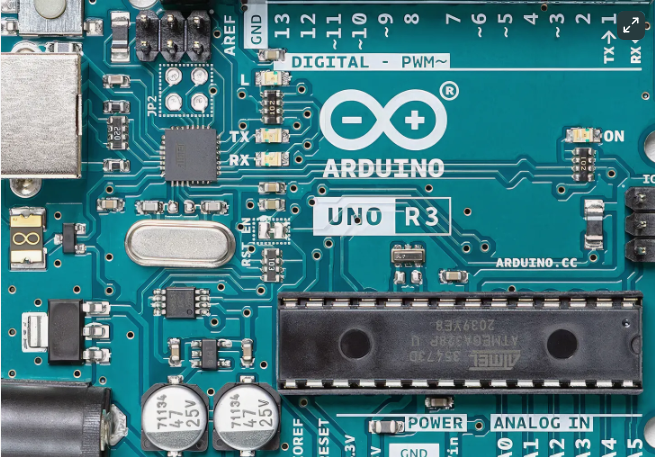
Close-up of Arduino Uno R3 product promotion map
In addition to becoming smaller, the most significant change is the application of copper paving-that is, filling the blank areas between traces on PCB through computer-generated areas.
Why did this design rise? A general answer is: in the field of high-speed electronics, this approach helps to improve signal integrity. This makes this method indispensable in cutting-edge applications such as smart phones or desktops. But obviously, we are not talking about such high-end scenes.
Another change is that in 1980s, the Federal Communications Commission (FCC) began to apply the 47 CFR Part 15 rule (radio frequency interference standard) to all kinds of computer equipment. So the so-called "certification industry" has emerged: the prototype needs to be sent to the certification laboratory, paying high RF test fees, and if it fails, it will have to bear additional costs and delays. Copper plating can effectively reduce RF radiation, so it is often used in advance just in case.
Last but not least, it is the aesthetic change of the industry: amateurs interact with each other and follow the industrial trend. Any unconventional or outdated PCB aesthetic design is often criticized, even though critics may not be able to clearly point out the design defects.
Don't worry, let's face the core question first: how does copper laying work?
First, insert a concept: common mode choke
In electronic circuits, although the flow of electrons is restricted by conductors, the energy transfer is not realized by particle collision, but by electromagnetic field. The electromagnetic field originates from carriers, but extends freely to the surrounding space.
Ferrite and other materials will respond to the external magnetic field through valence electron rearrangement, thus absorbing the energy of the surrounding field. If this magnetic field is generated by a nearby conductor, the current flow in the conductor will be temporarily blocked during the rearrangement of electrons in ferrite. This is because ferrite will react to the current in the conductor when it absorbs the energy of magnetic field. As ferrite absorbs more and more energy, it will eventually reach saturation, that is, it can't absorb more magnetic energy. But even in this case, if the current in the conductor changes, ferrite will still hinder these changes until a new equilibrium state is reached.
This is the standard inductance principle, which has a clever variant: common mode choke. Its basic form can be seen in some computer cables: tubular ferrite element wraps two wires in the same direction. The more compact version uses an annular magnetic core, and each conductor is wound several times:
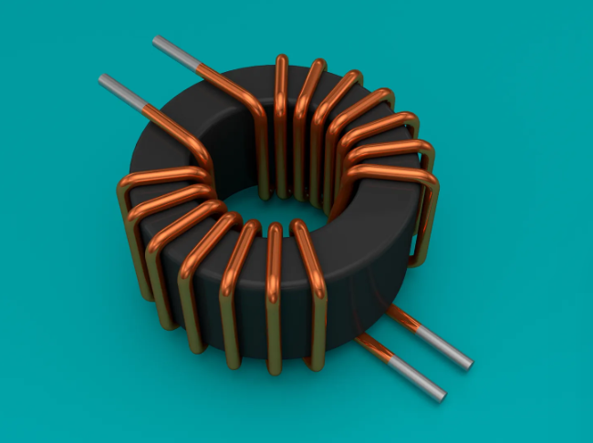
Schematic diagram of common mode choke coil
Common-mode current situation: When there is common-mode current flowing in the same direction in two wires, a consistent magnetic field will be generated to act on ferrite. This makes the device behave like an ordinary inductor. Direct current (DC) can pass smoothly, but for high-frequency alternating current (AC) components, it will weaken them according to the rate of frequency change (that is, it is proportional to AC frequency). This is because the inductance will produce inductive reactance to alternating current, and the higher the frequency, the greater the inductive reactance, thus hindering the passage of alternating current.
Differential mode current situation: On the contrary, if there are complementary currents flowing in opposite directions, such as differential signal pairs or "+"and "-"wires connected to the power supply, the generated magnetic fields will cancel each other out and the sum is zero. There is no magnetization phenomenon, and ferrite does not absorb energy, so the inductance of the device (a resistance-like index to measure its attenuation to AC signals) remains at a low level.
Common-mode choke can suppress RF interference on long cables: RF interference usually produces the same induced electromotive force in all bundled conductors, resulting in common-mode current. The common-mode choke can distinguish these common-mode currents from the differential signals we are concerned about, thus playing a role in suppressing RF interference on long cables.
Go back to laying copper
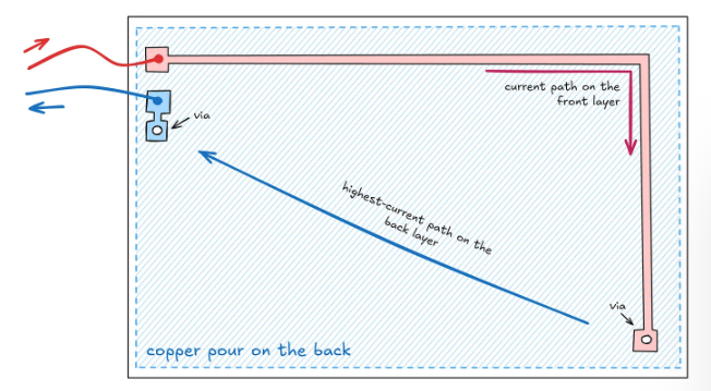
Inductance phenomenon is not limited to ferrite cores, but also exists in PCB traces (although the degree is slight). In order to let everyone understand why PCB routing inductance is important more intuitively, give a specific circuit board example. The structure of this circuit board is: there is a single red trace on the top floor, a blue copper plane on the bottom floor, and two vias to complete the connection of the whole circuit.
Schematic diagram of simple PCB structure
When a direct current (DC) signal is applied to the pins of the PCB, the "forward" current of the top layer is limited to the trace. In theory, the return current of the bottom layer can diffuse freely, but in practice it will choose the path with the least resistance, that is, the shortest straight path between two vias. This is because current always tends to flow along the path with the least impedance to minimize energy loss.
With the increase of sine wave frequency f, the magnetization-related quasi-resistance effect in the original current path will also increase. This is because PCB traces have inductance characteristics, and the inductance value L is usually between tens and hundreds of nanohenries, depending on the length of traces and other factors. For a given frequency f and inductance l, the formula of inductance is:
That is, at the sinusoidal frequency of 20MHz, the inductance can reach about 50Ω.
What survives is the compensation mechanism: if the bottom reflow path is close to the top routing projection path, it will form a state similar to a common mode choke-the magnetic fields cancel each other and the impedance remains low.
This will lead to two practical problems:
First, if the forward path is far away from the best available return path, it will produce higher impedance. In this case, more energy will be radiated to the surrounding space in the form of electromagnetic waves on the high-speed data line. This will not only lead to the loss of signal transmission, but also cause electromagnetic interference to the surrounding electronic equipment.
Secondly, if there are some irrelevant "victim" traces nearby, and these traces provide a path to return to ground (even through the body of the integrated circuit), then the current may choose this path instead of our carefully designed current path. This may lead to errors and instability in signal transmission, because the path of current is no longer what we expected.
Is it necessary to lay copper on the whole board?
Not necessarily. Laying copper is not the only solution, but this method can save time compared with manually laying current return channels for each data bus.
No matter which method is adopted, it needs careful design. For example, problems caused by discontinuous copper laying:
Discontinuous copper laying leads to inferior reflow path
Copper paving is also easy to ignore the problem of power wiring. For example, the Vdd power supply design in the upper right corner of the chip below is not very good.
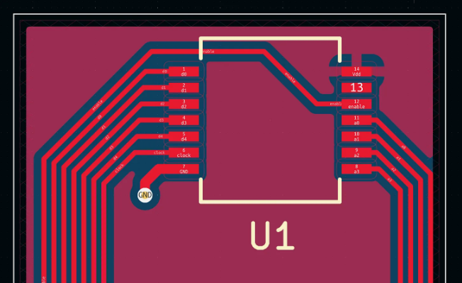
The positive power supply path is very long
In order to simplify the design, some enthusiasts will choose to use a four-layer board and dedicate the middle two layers to GND and Vdd. This scheme is effective, but the cost is doubled.
Another problem is that the power plane (or copper) can reduce the inductance of PCB, but it will increase the bypass capacitance of the whole PCB. For digital signals, the increased bypass capacitance is usually acceptable because it helps to stabilize the signal and reduce noise. However, in analog electronic circuits, especially in the feedback loop of operational amplifier (op-amp), every increase of bypass capacitance (such as several picofarads) may bring adverse effects.
In practical application, for most projects that use ESP32, Raspberry Pie or 8-bit AVR microcontroller, there is no need for excessive entanglement: copper laying should be based on convenient design, rather than blindly following network suggestions. The real challenge begins when dealing with high-speed interfaces such as MIPI-DSI and USB3.0.
About Maxipcb
Maxipcb empowers innovators to turn cutting-edge technologies into reality.
We offer one-stop solutions for design, simulation, testing, PCB manufacturing, component procurement and SMT assembly, enabling efficient development, rapid deployment and risk control across the full product lifecycle.
Serving the world in communications, industrial automation, aerospace, automotive, semiconductor and beyond, we build a safer, more connected future together.


