With the development of integrated circuits and related applications, the signal rate is getting higher and higher, which will double every 3-4 years. With the increase of signal rate, loss has become one of the most important factors affecting signal quality.
1. High-speed signal link loss analysisWith the development of integrated circuits and related applications, the signal rate is getting higher and higher, which will double every 3-4 years. With the increase of signal rate, loss has become one of the most important factors affecting signal quality.
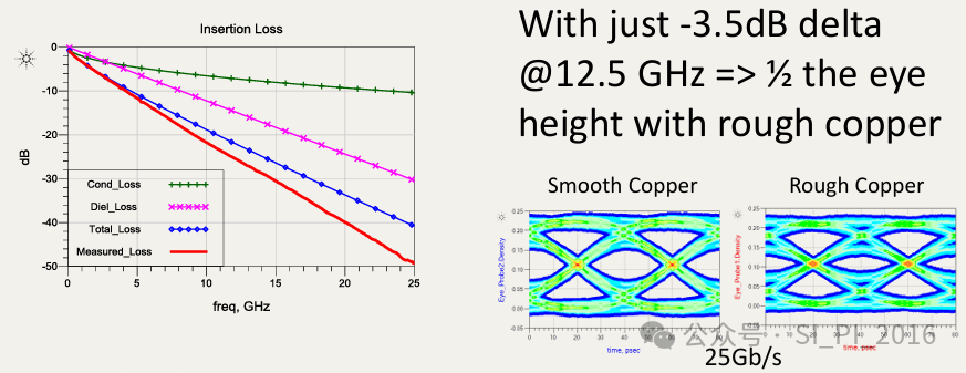
The total loss of the whole high-speed link = conductor loss+dielectric loss+radiation loss.
Generally speaking, we don't pay much attention to radiation loss from the perspective of SI, because as long as the impedance design of the system is not particularly outrageous, the radiation energy is usually controlled in a very small range, and the impact on the overall performance can be ignored.
Dielectric loss refers to the energy loss caused by the dielectric material when the signal passes through the PCB transmission line, which is generally expressed by Loss Tangent or Df(Dissipation Factor).
At present, the high-speed signal like serdes has reached the rate node of 112G/224G, and the improvement space of dielectric loss brought by PCB materials is getting smaller and smaller. At the same time, better PCB materials mean higher costs.
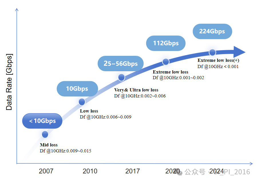
Therefore, many engineers focus on optimizing conductor loss.
The conductor loss is mainly caused by the resistance effect and scattering loss of metals. The resistance effect mainly refers to the resistance of the metal itself. At low frequencies, the current is evenly distributed inside the copper foil, and the loss is small. At high frequencies, the current will be distributed on the surface of the copper foil (the current flow will mainly be concentrated in the skin depth, as shown in the left figure below), and the cross-sectional area of the current will decrease, which will lead to the increase of the high-frequency resistance and thus the increase of the loss, which is often referred to as the skin effect.
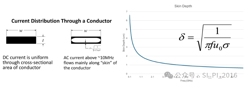
The skin depth related to skin effect is determined by frequency, and the copper thickness of transmission line is related to PCB technology, which has been determined at the beginning of design. Therefore, there is almost no good way to avoid the loss caused by skin effect at present, so how to reduce the conductor loss, the focus of industry is basically on the study of surface roughness.
2. Surface roughnessThe surface of PCB copper foil is not a complete plane. Microscopically, some particles can be seen. These particles will increase the contact area between copper foil and resin, make it more adhesive, and the copper skin is not easy to fall off. However, these particles will increase the conductor loss sharply at high frequency, which is called the surface roughness of copper foil.
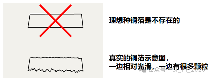
The surface roughness of copper foil originates from the material processing process [3]p.11, and its purpose is to increase the adhesion between copper foil and medium. Copper foil will have one side that is relatively flat and the other side that is relatively rough. [2]p.22
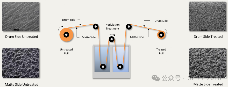
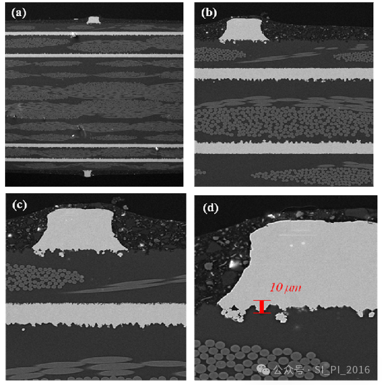
In order to make copper foil adhere to dielectric material (FR4, glass fiber woven plate) by hot pressing, the interface between copper foil and FR4 is usually rough. [3]p.10,12
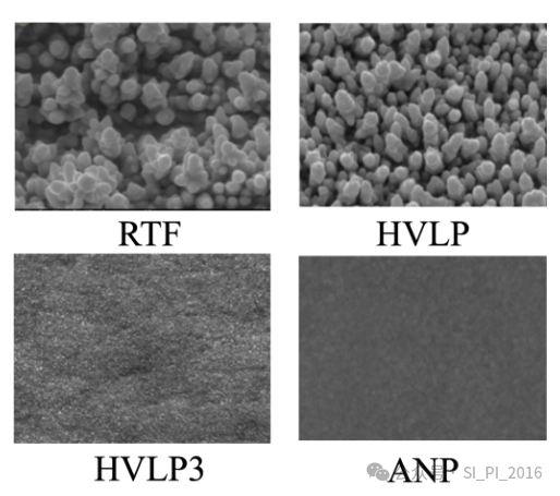
Ra and Rz are commonly used in engineering to represent the surface roughness of copper skin. According to the performance of different copper sheets, they are divided into different grades, including RTF(Reverse Treated Foil), VLP(Very Low-Profile), HVLP (high very low-profile), ANP(Any No-Profile) and so on.
At present, the most advanced copper foil in the industry is HVLP5, which has almost no Rz, which can reduce the surface roughness a lot! However, CCL and PCB factories are still trying to overcome the influence of copper foil without particles on material Peeling.
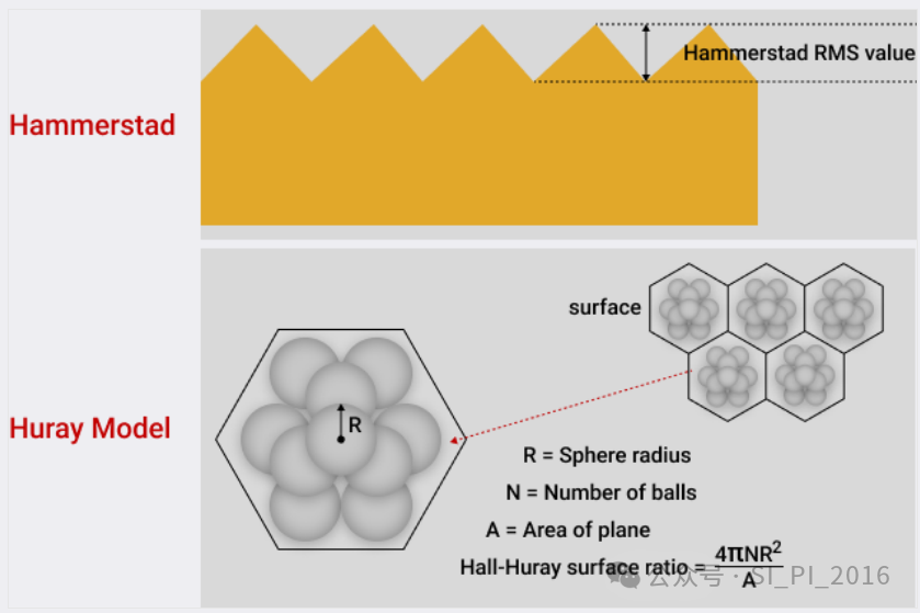
Generally, two models are used to characterize the roughness of copper foil in the industry. The first model is Hammerstad model, as shown in the following figure. This model uses the height of copper teeth of copper foil to characterize roughness.
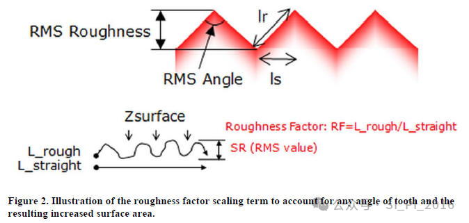
Although Hammerstad model only needs RMS parameters of sawtooth texture profile, it has no physical significance, but is a function obtained from fitting insertion loss curve. Based on the real physical structure of copper foil, the Huray model equates the rough particles on the surface of copper foil with a uniform sphere as shown in the following figure, calculates the power loss according to the absorbed power and scattered power after passing through the sphere, and derives the roughness formula, which fits the actual situation better and has physical significance.
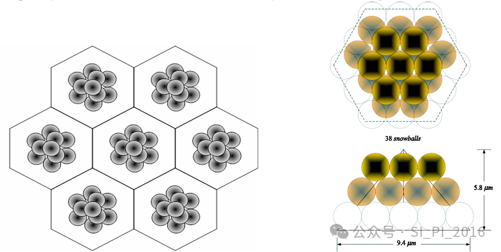
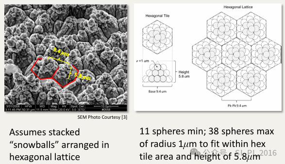
At present, the mainstream EDA software mainly uses Huray model to characterize the roughness of copper foil, and its parameters mainly include snowball radius and the ratio of snowball surface area to pile bottom area (surface ratio).
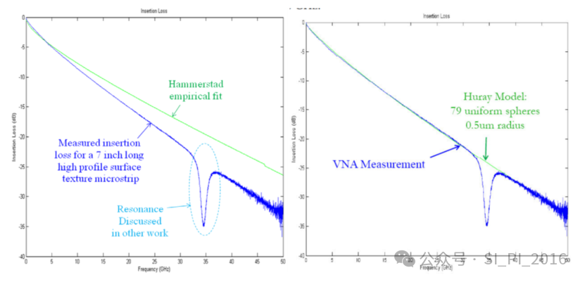
People often ask which model is better. Generally speaking, for low roughness, the effect of Hammerstad model and Huray model is similar [4] P.10,15. However, the maximum function of Hammerstad model is 2, but in practice, the power loss affected by surface roughness can be more than 2 times, so Hammerstad model is suitable for low roughness (HRMS<2um) and low frequency scenes, while Huray model is suitable for general processes and broadband scenes. The following figure shows the results of fitting a section of 7inch transmission line with rough surface with Hammerstad model and Huray model respectively. At low frequency, both of them fit the measured data well, while at high frequency, the accuracy of Hammerstad model is obviously not as good as that of Huray model [3].
 3. Detu copper foil surface roughness solution
The surface roughness of copper foil has a great influence on the loss of high-speed signal. The following figure shows the insertion loss of a 4-inch microstrip line simulated by using SonicPCB, a pre-simulation tool of Detu Technology. The green curve is the result of smooth condition, and the red curve is the result of Huray model with snowball radius of 0.3um and surface ratio of 1.8. By analyzing the image, it can be seen that the roughness has a great influence on the insertion loss of transmission lines, and the difference between them is close to 3dB at 50GHz. With the increase of signal transmission rate and frequency, the loss caused by roughness will become more and more obvious, so the industry urgently expects a simple and effective roughness extraction scheme.
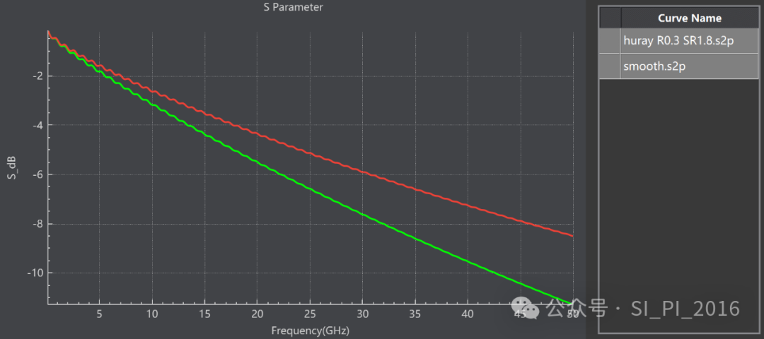
At present, there is no reliable tool in the market to accurately extract the roughness, and it is more common to measure the Rz and Ra of the rough surface with instruments to characterize the roughness. However, when analyzing transmission line loss, Rz and Ra can only be applied to Hammerstad model, but not to more accurate Huray model. At the same time, the accuracy of Rz and Ra will also be affected by measuring equipment, and high-precision equipment is often expensive.
In order to solve this problem and demand, the technical team of Ningbo Detu Technology, together with Intel and several copper foil manufacturers, jointly developed SRTool, a tool for extracting the surface roughness of copper foil. The tool reads the copper foil slice through the image algorithm and generates the corresponding surface contour line. Then, a rough 3D model is established by using the probability distribution method for simulation, and the influence of roughness on transmission line loss is analyzed and a Huray model is generated to characterize the roughness of copper foil.
3.1 Operation process:
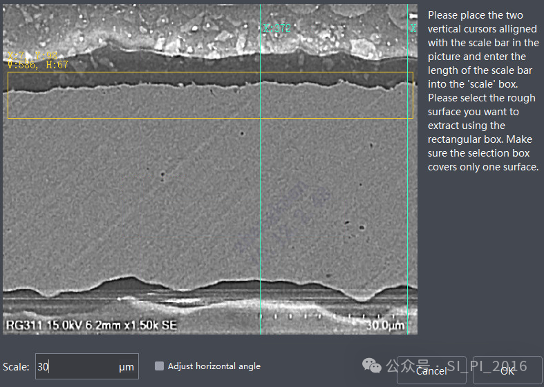
(1) Import copper foil slice, read rough surface and generate Profile. SRTool supports material library to manage different rough data.
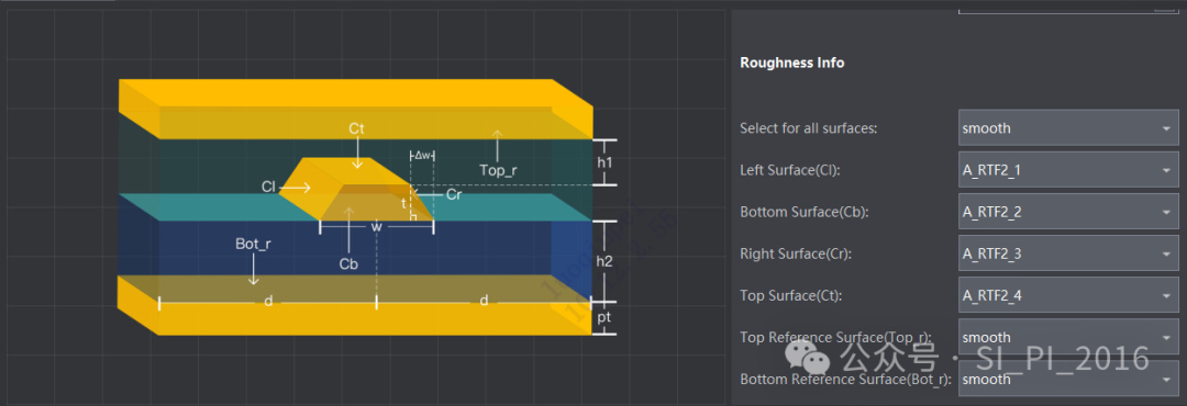
(2) Apply the rough data to all surfaces of the transmission line model, including the transmission line up and down, left and right, and the upper and lower reference ground.
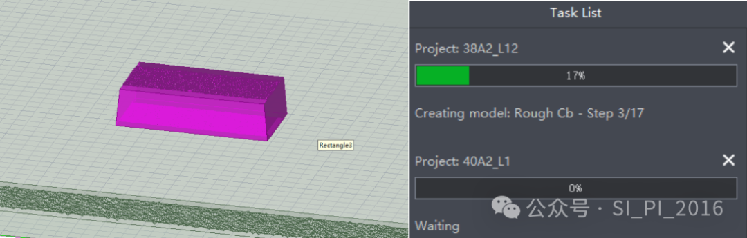
(3)SRTool automatically runs the 3D modeling simulation script, just waiting for the simulation to be completed.
(4) After the simulation is completed, SRTool automatically reads the simulation results, analyzes and generates the Huray model.
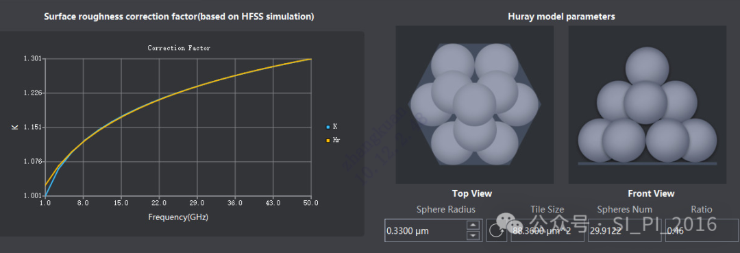
(5) Put the results of SRTool (Huray model parameters) into transmission line simulation software, such as SonicPCB, and further analyze the impedance and S parameters of transmission line.
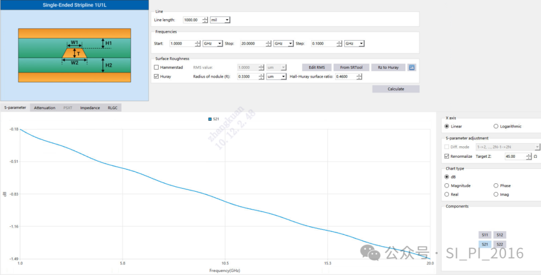
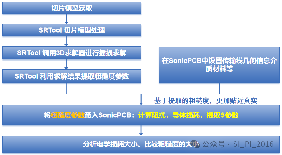
This process can obtain the real surface roughness of copper foil from PCB slices in one stop, and it can be directly applied to the solution of S parameters of transmission lines. It can make the SI/PI engineer of the end customer quickly and accurately judge the influence of copper foil roughness on the loss, distinguish the roughness grade of copper foil suppliers and evaluate whether the material selection of copper foil is reasonable.
The concise flow chart is as follows:
3.2 Software advantages
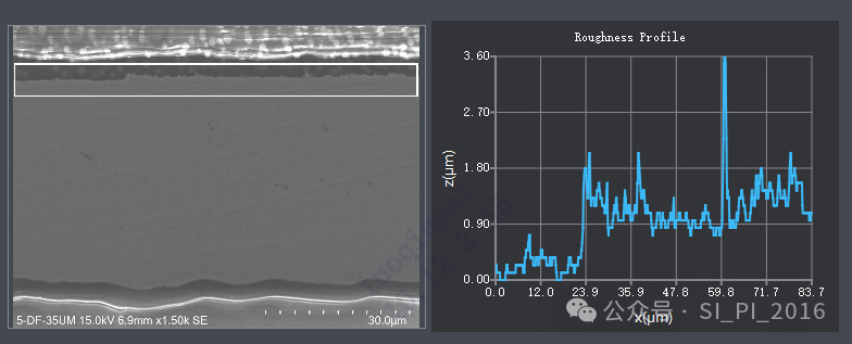
(1) The original input data of the model comes from the slice diagram, which is more realistic.
The height distribution map on the right accurately expresses the ups and downs of the slice.
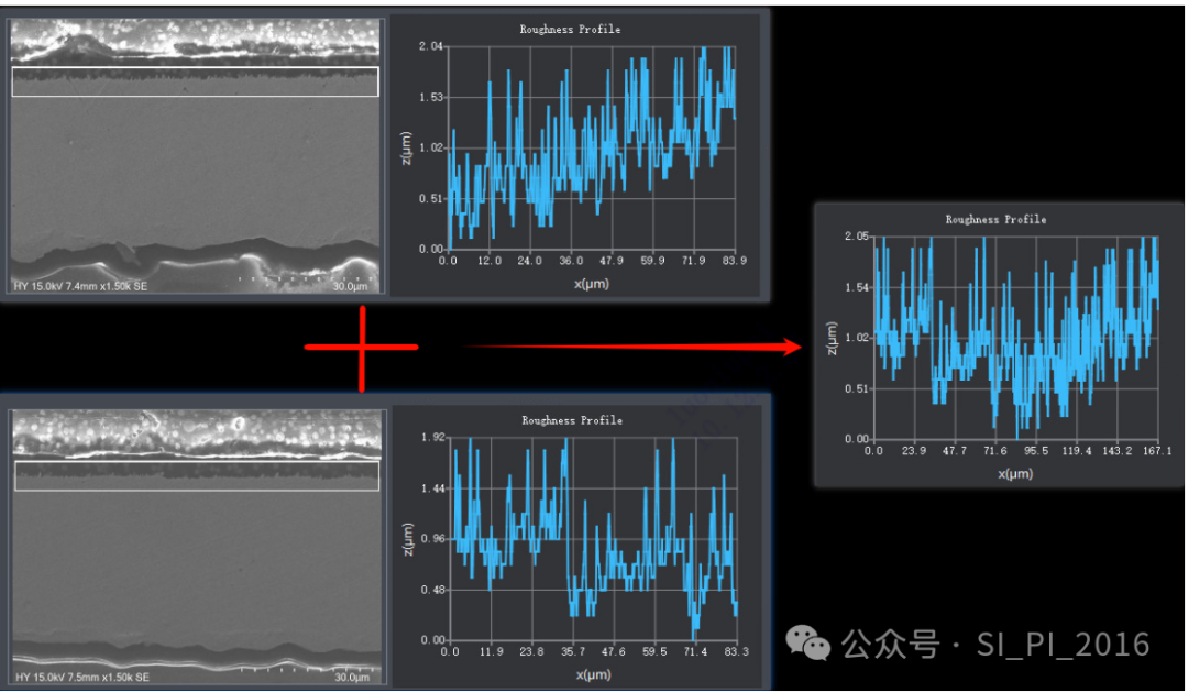
(2) provide the Merge function of different slices of the same copper foil, so as to reduce the error caused by the consistency of slices.
The two slices in the following figure were originally an upward trend and a downward trend, respectively. After the Merge, the height distribution tends to be horizontal, but the height trend of the original synthetic data is well preserved.
(3) Using 3D transmission line model simulation, the roughness of different surfaces is set respectively, which is close to the application scene.
You can select the imported slice data through the drop-down box on the right, then set different faces of the transmission line respectively, and finally send them to the 3D simulation solver for solution.
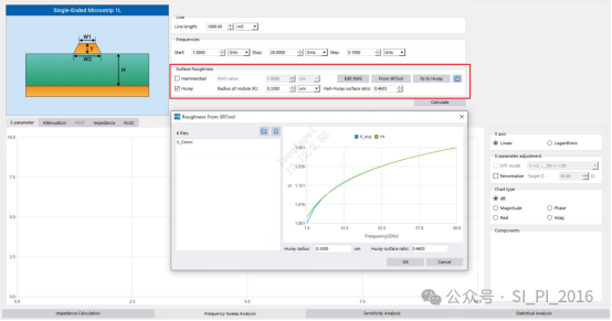
(4) Obtaining the roughness model parameters recognized by the industry, which is convenient for application in simulation software.
Parameters of Huray model can be obtained and exported as CSV data. Then input Huray model parameters in SonicPCB, our pre-imitation tool, or import CSV and simulate.
(5) The operation is simple, the 3D model can be generated automatically, and multiple roughness extraction tasks can be submitted and executed in sequence.
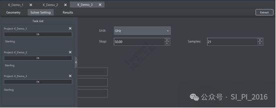
Solving supports multiple tasks. After clicking Export, the software will solve them in turn according to the task queue.
3.3 Application case
There have been many successful cases of this set of roughness extraction process of SRTool. The following is a real case of a customer, with four slices of copper foil, as shown in the figure below.
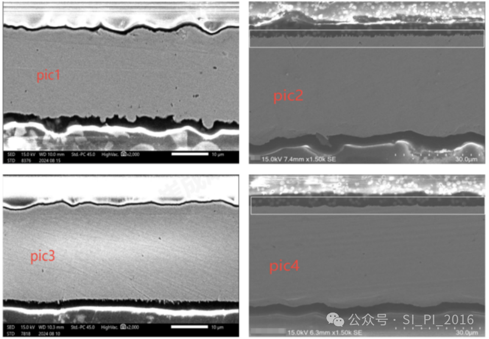
Use SRTool to extract the Profile of the above four slices, as shown in the following figure.
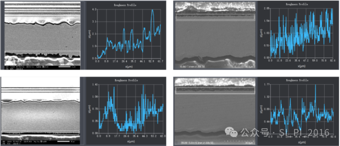
From the above images, it can be found that the Rz Ra of the profile in pic1 is large, while the peak-to-peak spacing in pic2 is small, so it can be roughly judged that the roughness of these two copper foils is relatively large.
According to the above-mentioned process, the roughness is extracted, and the roughness of four cases is applied to a section of 8inch transmission line in SonicPCB to obtain the insertion loss curve, as shown in the following figure.
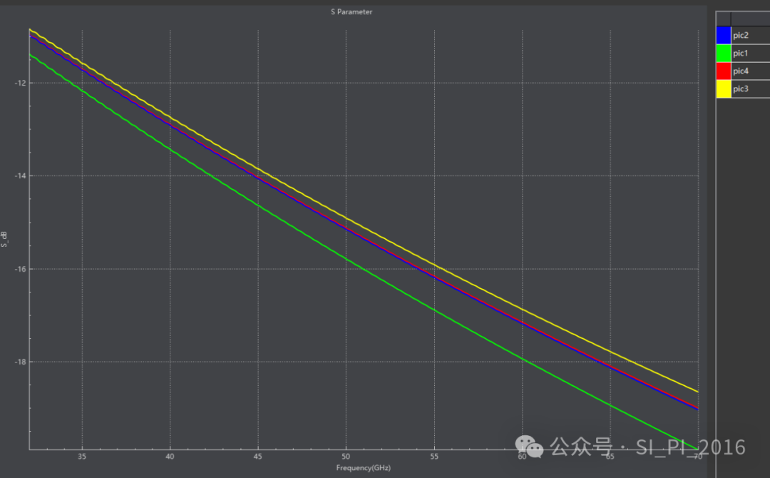
According to the image, it can be intuitively judged which copper foil brings less loss, which is consistent with the previous rough judgment based on profile.
And it can be seen from the image that the difference of insertion loss caused by different roughness is more than 1dB at higher frequency. Therefore, in high-speed and high-frequency scenes, the roughness factor can not be ignored. For the same transmission line structure, copper foils with different roughness may also bring great loss differences.
At present, the analysis results of this process have completed several groups of experimental data, and a large number of board tests have been carried out in conjunction with a number of copper foil manufacturers, and reasonable and recognized results have been obtained by many experts. SRTool and SonicPCB have also been put into commercial application and have been tested and recognized by many large manufacturers, and interested partners can try out the evaluation.
About Maxipcb
Maxipcb empowers innovators to turn cutting-edge technologies into reality.
We offer one-stop solutions for design, simulation, testing, PCB manufacturing, component procurement and SMT assembly, enabling efficient development, rapid deployment and risk control across the full product lifecycle.
Serving the world in communications, industrial automation, aerospace, automotive, semiconductor and beyond, we build a safer, more connected future together.

