With the rapid development of electronic technology, various electronic products have permeated every aspect of our lives, and LCD screens are one of the most widely used components. They are extensively applied in mobile phones, computers, meters, controllers, and other electronic devices. Currently, the mainstream LCD display interfaces include RGB, LVDS, MIPI, and HDMI, all of which involve high-speed signal transmission in practical applications.
1. Preface
With the rapid development of electronic technology, various electronic products have permeated every aspect of our lives, and LCD screens are one of the most widely used components. They are extensively applied in mobile phones, computers, meters, controllers, and other electronic devices. Currently, the mainstream LCD display interfaces include RGB, LVDS, MIPI, and HDMI, all of which involve high-speed signal transmission in practical applications.
Signal transmission impedance is a crucial factor that must be considered in circuit design, especially for differential signals and high-speed transmission signals. If impedance matching is properly achieved, it can not only ensure smooth signal transmission on the transmission line, reduce signal reflection, and improve signal integrity and accuracy but also effectively suppress noise interference, thereby laying a solid foundation for the EMC (Electromagnetic Compatibility) performance of the entire product.
2. Impedance Matching
Impedance matching refers to a working state where the load impedance is adapted to the internal impedance of the excitation source, so as to achieve maximum power output and optimal signal transmission effect. This is particularly critical for high-speed digital interfaces, as impedance mismatch will directly affect signal quality and system stability.
High-speed digital interfaces such as HDMI, LVDS, and FPD-Link have strict requirements for impedance control. In practical PCB design, the matching of characteristic impedance can be realized by adopting specific transmission line structures (such as microstrip lines and striplines) and precisely controlling PCB wiring parameters (including line width, line spacing, and dielectric thickness), thereby ensuring the stable transmission of high-speed digital signals and avoiding signal distortion caused by impedance mismatch.
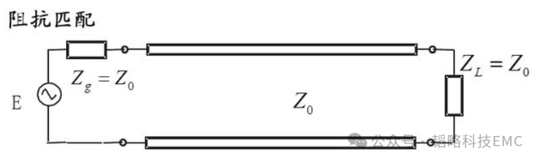
Figure 1 Impedance matching
【Functions of Impedance Matching】
-
Reduce crosstalk between signals;
-
Minimize signal reflection on the transmission line;
-
Ensure the long-term stability and reliability of the system;
-
Meet the standards and technical requirements of high-speed signal transmission.
【Implementation Methods of Impedance Matching】
-
Transformer matching: Suitable for scenarios requiring impedance conversion and isolation;
-
Series/parallel resistor matching: A simple and cost-effective method, widely used in high-speed digital interfaces;
-
Adjusting the characteristic impedance of the transmission line: Achieved by optimizing PCB wiring parameters and transmission line structure.
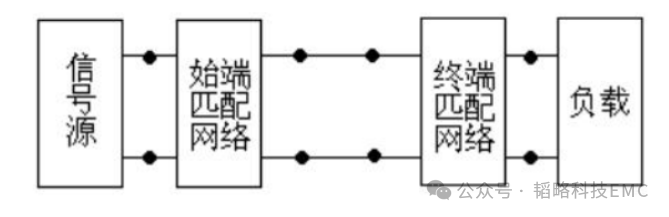
Fig. 2 Method of impedance matching
3. cases analysis and rectification
In an actual EMC test, it was found that the product failed the RE (Radiated Emission) test. From the test data shown in Figure 4, it can be clearly observed that the clock harmonics exceeded the standard significantly. Through analysis of the test data, it was determined that the over-standard fundamental frequency was approximately 73.75MHz. Using a spectrum analyzer to trace the source of the over-standard clock signal, it was diagnosed that the problem originated from the differential signal clock of the LCD screen, which was caused by impedance mismatch of the differential signal.
Rectification Measures: A 100Ω resistor was connected in parallel between the differential signals at the load end to achieve impedance matching. The specific rectification measures are shown in the following figure:
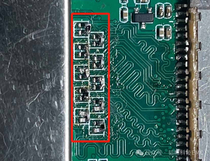
Figure 3 pictures of actual rectification measures
After adding the parallel resistor to form impedance matching, the RE test was performed again. The test results showed that impedance matching significantly improved the RE radiation effect, with a maximum noise reduction of 14dB. The test data before and after rectification are shown in the following figures:
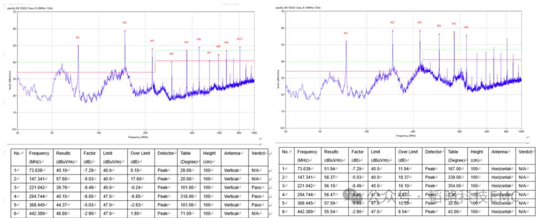
Figure 4 RE test data before rectification
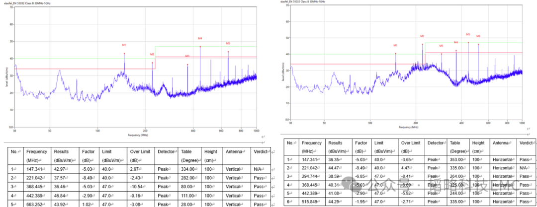
Figure 5 RE test data after rectification
4. Summary
Impedance matching is a key focus in high-speed signal circuit design. Impedance mismatch will not only lead to signal crosstalk and damage signal integrity but also generate noise interference to the entire PCB. This interference will further cause the product’s radiated emission to exceed the standard, resulting in failure to pass the EMI (Electromagnetic Interference) test.
Therefore, the impedance matching of high-speed transmission circuits must be fully considered in the design stage. Only when the "perfect" matching between the output impedance of the signal source and the load impedance is achieved can the signal be transmitted without reflection, the maximum power utilization be realized, and the EMC performance of the product be effectively guaranteed, ensuring that it meets the relevant test standards.
About Maxipcb
Maxipcb empowers innovators to turn cutting-edge technologies into reality.
We offer one-stop solutions for design, simulation, testing, PCB manufacturing, component procurement and SMT assembly, enabling efficient development, rapid deployment and risk control across the full product lifecycle.
Serving the world in communications, industrial automation, aerospace, automotive, semiconductor and beyond, we build a safer, more connected future together.


