To achieve a good electromagnetic compatibility (EMC) design for high-speed backplanes, printed circuit boards (PCBs) must meet EMC and susceptibility standards during normal operation. Proper layer stacking helps shield and suppress electromagnetic interference (EMI).
1 Layer Stacking of High-Speed Backplanes
To achieve a good electromagnetic compatibility (EMC) design for high-speed backplanes, printed circuit boards (PCBs) must meet EMC and susceptibility standards during normal operation. Proper layer stacking helps shield and suppress electromagnetic interference (EMI).
The EMC analysis of multilayer PCBs can be based on Kirchhoff's laws and Faraday's law of electromagnetic induction.
According to Kirchhoff's laws, the transmission of any time-domain signal from the source to the load must follow a path with the lowest impedance (see Figure 1). In the figure, I=I′, with equal magnitude and opposite direction. I is defined as the signal current, I′ as the image current, and the layer where I′ is located as the image plane layer. If a power plane (POWER) is beneath the signal current, the image current loop is formed through capacitive coupling (see Figure 2).
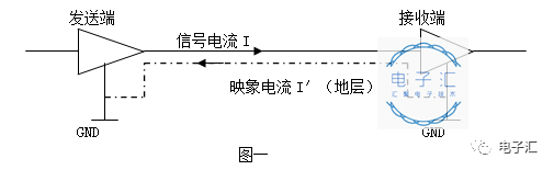
Signal current and image current (ground plane) at the transmitting and receiving ends
Based on Faraday's law of electromagnetic induction, the formula is as follows:
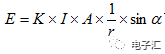
It can be concluded that the larger the value of A, the larger the value of E (see Figure 3).
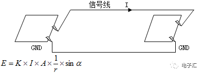
Schematic diagram of the relationship between signal line, ground and induced electromotive force E
Based on the above two laws, the following basic principles should be followed in the layer stacking of multilayer PCBs:
- The power plane should be placed as close to the ground plane as possible and beneath the ground plane.
- Wiring layers should be adjacent to the image plane layer.
- The power and ground planes should have the lowest impedance. The power impedance Z0 is related to the distance D between the power and ground planes and the area W of the planes.
- Striplines are formed in the inner layers and microstrip lines on the surface layers, with different characteristics for each.
- Important signal lines should be immediately adjacent to the ground plane.
1.1 Six-layer PCBs
Table 2 Layer Stacking Schemes for Six-layer PCBs
| Scheme |
Layer 1 |
Layer 2 |
Layer 3 |
Layer 4 |
Layer 5 |
Layer 6 |
| A |
S1 |
GND |
S2 |
S3 |
POWER |
S4 |
| B |
S1 |
S2 |
GND |
POWER |
S3 |
S4 |
| C |
S1 |
GND |
S2 |
POWER |
GND |
S3 |
| D |
GND |
S1 |
POWER |
GND |
S2 |
GND |
Scheme D is recommended for backplane design, which offers the optimal EMI performance among six-layer PCB schemes.
1.2 Eight-layer PCBs
Table 3 Layer Stacking Schemes for Eight-layer PCBs
| Scheme |
Layer 1 |
Layer 2 |
Layer 3 |
Layer 4 |
Layer 5 |
Layer 6 |
Layer 7 |
Layer 8 |
| A |
S1 |
S2 |
S3 |
GND |
POWER |
S4 |
S5 |
S6 |
| B |
S1 |
GND |
S2 |
S3 |
S4 |
S5 |
POWER |
S6 |
| C |
S1 |
GND |
S2 |
S3 |
GND |
POWER |
S4 |
S5 |
| D |
S1 |
GND |
S2 |
GND |
S3 |
POWER |
S4 |
S5 |
| E |
S1 |
GND |
S2 |
GND |
POWER |
S3 |
GND |
S4 |
For eight-layer PCBs with 5 signal layers, Scheme D is the best choice, where S1, S2 and S3 are all excellent wiring layers and the power plane impedance is relatively low. For eight-layer PCBs with 4 signal layers, Scheme E in Table 3 is optimal, with every signal layer being a good wiring layer. In all these schemes, adjacent signal layers should be used for wiring.
1.3 Ten-layer PCBs
Table 4 Layer Stacking Schemes for Ten-layer PCBs
| Scheme |
Layer 1 |
Layer 2 |
Layer 3 |
Layer 4 |
Layer 5 |
Layer 6 |
Layer 7 |
Layer 8 |
Layer 9 |
Layer 10 |
| A |
S1 |
GND |
S2 |
S3 |
GND |
POWER |
S4 |
S5 |
GND |
S6 |
| B |
S1 |
GND |
S2 |
GND |
S3 |
GND |
POWER |
S4 |
GND |
S5 |
| C |
S1 |
GND |
S2 |
S3 |
GND |
POWER |
S4 |
GND |
S5 |
GND |
| D |
GND |
S1 |
S2 |
GND |
S3 |
S4 |
GND |
POWER |
S5 |
GND |
Schemes C and D are generally used for backplanes in ten-layer PCBs. Scheme D provides better EMC shielding performance than Scheme C, but its drawback is the adjacent signal layers, which require careful wiring.
In summary, PCB layer stacking is a complex task that needs to consider multiple factors.
2 Wiring of High-Speed Backplanes
The wiring of high-speed signals mainly focuses on signal integrity, including delay, reflection, crosstalk, simultaneous switching noise (SSN) and electromagnetic compatibility (EMI).
2.1 Clock Signal Lines
Clock signal lines need to consider both signal integrity and EMI issues, and their design directly determines the performance of high-speed backplanes.
Clock signal lines are generally routed in the inner layers of the backplane, preferably sandwiched between two plane layers. The impedance of the wiring must be controlled, and impedance consistency should be ensured when switching between different layers to prevent the impact of signal reflection on the clock.
The spacing between clock signal lines and other lines should meet the 3W principle at a minimum, which can effectively prevent crosstalk caused by clock lines. For signal lines with synchronous timing requirements, equal-length wiring is required in the design to avoid the impact of wiring delay on synchronous timing.
2.2 High-Speed Data Signal Lines
High-speed data signal lines mainly focus on signal integrity issues such as impedance control, reflection and crosstalk.
High-speed signal lines are generally routed in the inner layers of the backplane and adjacent to the ground plane. The wiring impedance must be controlled, and impedance consistency should be ensured when switching between different layers to prevent signal reflection caused by impedance mismatch, which would lead to overshoot and ringing on the data lines and affect data reliability.
The spacing between high-speed signal lines and other lines should meet the 2W principle at a minimum, or the 3W principle if wiring conditions permit, which can effectively prevent mutual crosstalk between data lines and ensure data reliability. Parallel data signal lines with synchronous timing requirements must be strictly equal in length to avoid the impact of wiring delay on the synchronous timing of data lines.
2.3 LVDS Wiring
Edge Rate: For the backplane bus structure in Multi-Point mode, the Time Domain Reflectometry (TDR) analysis method proposed by North East Systems Associates (NESA) is usually used to describe the impact of signal edge rate. The signal transition time (rise and fall time) is a crucial indicator for transmission line calculation. It should be noted that the Multi-Point and Multi-Drop bus structures cannot be used when the signal edge rate is less than 300ps.
Stub Length: The impact of stub length on the backplane bus is generally measured by the TDR and Time Domain Transmission (TDT) "Passive Signal Integrity" methods proposed by NESA. The general conclusion is that the longer the stub length, the more severe the impedance discontinuity on the line; the more severe the impedance discontinuity, the larger the amplitude of damped oscillation at the rising and falling edges of the signal. Therefore, the shorter the stub length on the single board, the smaller the impact on the backplane bus.
Placement of Interface Devices: To reduce the impact of stub length on the transmission lines on the backplane, the stub length should be minimized. Therefore, in the layout of the single board, the position of interface devices should be determined first to ensure the shortest stub length. Bus transceivers (Multi-Point mode) or receivers (Multi-Drop mode) should be placed as close to the connector as possible, preferably on both sides of the board, to reduce the stub length.
Differential Impedance: BLVDS requires a differential impedance of 100 ohms between a pair of differential lines. If a spacing of 20mil is maintained between two pairs of differential lines, the mutual common-mode and differential-mode interference can be neglected. The closer the spacing between a pair of differential lines, the less radiated interference they emit to the outside; the interference from the outside to the pair of differential lines is reflected as a smaller differential-mode component and a larger common-mode component at the receiving end, which is obviously beneficial for the receiver.
If W represents the wiring width, d the thickness of the interlayer electrolyte, l the spacing between a pair of differential lines, and L the spacing between differential line pairs:
- A wider W makes it easier to process the characteristic impedance of the PCB accurately; the wiring width on the backplane is generally 12mil.
- d should not be too small (a smaller d leads to lower characteristic impedance); the electrolyte thickness between signal layers or between signal and ground layers on the backplane should not be less than 13mil.
- l should be at least larger than d; generally, l is at least 18mil when d is 13mil.
- L should generally be larger than twice the value of l.
Bus Termination: For Multi-Point bus, matching resistors should be installed at both ends. For Multi-Drop bus, one or two matching resistors should be used according to the position of the driver. The resistance value should be consistent with the effective impedance of the line after loading. The general principle is to select a matching resistor with a value slightly larger than the actual effective resistance (rather than smaller). A slightly larger resistance only causes adverse reflection effects, while a smaller resistance will reduce the signal amplitude.
Stub Termination: A series resistor of 15 to 30 ohms should be connected in series with each signal line of the LVDS differential signal pair near the connector pins (see Figure 1), which can filter the edge rate and effectively suppress the damped oscillation caused by the stub and edge rate. This can also be achieved by connecting a small capacitor across the two input ends of the differential receiver, but the capacitance value is difficult to control, so resistors are generally used. This method is only applicable to Multi-Drop wiring and is particularly effective for Multi-Drop wiring with fast edge rates and long stub lengths.
Connector and Pin Assignment: The selection of connectors depends on different applications, generally considering factors such as the number of signal pins, mechanical size requirements, electrical performance requirements, and pin arrangement requirements. In general, the fewer the pins per row of the connector, the better. For most connectors, a pair of differential signals should be placed in the same row to ensure the same wiring length. Other TTL/CMOS signals should be separated from LVDS signals to avoid mutual radiated interference. Special pin-length pins should be used for power and ground to ensure the power-on sequence. The typical power-on sequence is ground → power → I/O lines, and the power-off sequence is the reverse: I/O lines → power → ground.
Line Pair Balance: Unbalance between differential line pairs will introduce common-mode noise. The best way to control common-mode noise is to ensure that the two lines of the differential line pair are as equal in length as possible, consistent in wiring mode, and keep a constant spacing between them, thus achieving a balanced state. In addition, different lengths of the two signal lines in a differential pair will cause not only skew but also jitter at the receiving end, both of which need to be paid close attention to. It is also important to avoid the total length of a signal line being an integer multiple of a quarter of the signal wavelength.
2.4 PCB Design Method Based on Signal Integrity Analysis
A PCB design method based on signal integrity (SI) analysis is recommended for high-speed backplane wiring, with the following design process:
- Establish a signal integrity model for high-speed digital signal transmission before PCB design.
- Conduct a series of pre-analyses of signal integrity issues based on the SI model, and select appropriate component types, parameters and circuit topologies as the basis for circuit design according to the simulation and calculation results.
- During the circuit design process, submit the design scheme to the SI model for signal integrity analysis, and calculate and analyze the solution space of the design scheme by integrating the tolerance ranges of component and PCB parameters, and possible topology and parameter changes in PCB layout design.
- After the circuit design is completed, all high-speed digital signals should have a continuous and achievable solution space (i.e., the signal integrity requirements can still be met when PCB and component parameters change within a certain range, and the layout of components and wiring of signal lines on the PCB have a certain flexibility).
- Before the start of PCB layout design, take the obtained boundary values of each signal's solution space as the constraint conditions for layout design, which serve as the basis for PCB layout and wiring.
- During the PCB layout design process, submit the partially or fully completed design back to the SI model for post-design signal integrity analysis to verify whether the actual layout design meets the expected signal integrity requirements. If the simulation results fail to meet the requirements, the layout design or even the circuit design needs to be modified, which can reduce the risk of product failure caused by improper design.
- Fabricate the PCB after the design is completed; the tolerance range of PCB manufacturing parameters should be within the solution space of the signal integrity analysis.
- After the PCB is manufactured, use instruments for measurement and debugging to verify the correctness of the SI model and SI analysis, which serves as the basis for model modification.
On the basis of a correct SI model and analysis method, the PCB usually requires no or only a small number of repeated design modifications and fabrications to finalize the design, thus shortening the product development cycle and reducing development costs.
2.5 Layout and Materials of High-Speed Backplanes
The layout of high-speed backplanes should follow the principles of separating analog and digital areas and separating high-speed, medium-speed and low-speed areas to prevent analog-digital interference and crosstalk between signals. More ground pins should be defined on the vertical pins of the connector, which can provide the shortest return path for signals and prevent signal crosstalk. The processing of analog ground and digital ground on the backplane generally follows the principle of partition without separation: analog and digital signals are wired in their respective areas, and unrelated signal lines are not wired across areas.
High-speed backplanes must use high-speed connectors that meet the requirements according to the actual signal bandwidth, such as MOLEX's VHDM series connectors, which can meet the requirements of 3.125G and above. Derating design must be considered for connectors.
About Maxipcb
Maxipcb empowers innovators to turn cutting-edge technologies into reality.
We offer one-stop solutions for design, simulation, testing, PCB manufacturing, component procurement and SMT assembly, enabling efficient development, rapid deployment and risk control across the full product lifecycle.Serving the world in communications, industrial automation, aerospace, automotive, semiconductor and beyond, we build a safer, more connected future together.


