Precision PCB Fabrication, High-Frequency PCB, High-Speed PCB, Standard PCB, Multilayer PCB and PCB Assembly. The most reliable PCB&PCBA custom service factory
Precision PCB Fabrication, High-Frequency PCB, High-Speed PCB, Standard PCB, Multilayer PCB and PCB Assembly. The most reliable PCB&PCBA custom service factory
Home > News > PCB DESIGN > Master the Analysis of 4 Classic Operational Amplifier Circuits Quickly
Master the Analysis of 4 Classic Operational Amplifier Circuits Quickly
Circuits composed of operational amplifiers are referred to as op-amp circuits for short.
Apr 3rd,202636 Views
Operational Amplifier Circuits
Circuits composed of operational amplifiers are referred to as op-amp circuits for short.
There is a wide variety of such circuits, which are an important part of learning analog electronic technology and a must-master circuit for electronic engineers. With so many types of op-amp circuits, is it enough to just memorize them all?
No! Circuits are always changing, and it would be meaningless if you get stuck when the circuit configuration changes. The right way to learn is to understand and digest the underlying principles.
When analyzing the working principle of an op-amp circuit, first forget about inverting amplification, non-inverting amplification, adders, subtractors, differential inputs... and temporarily set aside the input-output relationship formulas... These will only confuse you. Also, ignore circuit parameters such as input bias current, common-mode rejection ratio, and offset voltage for the time being—these are considerations for circuit designers. We only need to understand the ideal operational amplifier, as this understanding is sufficient for most practical applications.
Schematic diagram of op-amp basic pins
In fact, two key rules can solve most op-amp problems, and these rules are clearly stated in all op-amp circuit textbooks: virtual short and virtual open. However, mastering their flexible application requires solid foundational knowledge.
Based on these two principles, we will quickly grasp the analysis method of op-amp circuits through 4 classic circuit examples!
About Virtual Short and Virtual Open
The open-loop voltage gain of an operational amplifier is extremely high—generally, the open-loop voltage gain of a general-purpose op-amp is above 80dB. Meanwhile, the output voltage of an op-amp is limited, usually ranging from 10 V to 14 V. Therefore, the differential input voltage of the op-amp is less than 1 mV, and the two input terminals are approximately at the same potential, which is equivalent to a "short circuit". The higher the open-loop voltage gain, the closer the potentials of the two input terminals are. We can understand the concept of virtual short through this reverse deduction.
Virtual Short: When analyzing an operational amplifier operating in the linear region, the two input terminals can be regarded as having the same potential. This characteristic is called false short circuit, or virtual short for short. Obviously, the two input terminals cannot be truly short-circuited. (The differential input voltage is no more than 1 mV)
How to understand Virtual Open? The differential input resistance of an op-amp is very large—generally, the input resistance of a general-purpose op-amp is above 1 MΩ. Therefore, the current flowing into the op-amp input terminals is often less than 1 μA, much smaller than the current in the external circuit of the input terminals. Thus, the two input terminals of the op-amp can usually be regarded as an open circuit, and the larger the input resistance, the closer the two input terminals are to an open circuit.
Virtual Open: When analyzing an op-amp operating in the linear region, the two input terminals can be regarded as an equivalent open circuit. This characteristic is called false open circuit, or virtual open for short. Obviously, the two input terminals cannot be truly open-circuited. (Assumed infinite differential input resistance)
Now that the concepts are introduced, let's test this theory with several examples to see how effective it is!
Case 1: Inverting Amplifier
Schematic diagram of the inverting amplifier circuit, including op-amp with ±15V power supply, input Vin, resistors R1 and R2, output Vout, and labeled nodes V- (inverting input) and V+ (non-inverting input, grounded)
Analysis of the circuit above:
According to the virtual short principle: the non-inverting terminal of the op-amp is grounded (0V), and the inverting terminal is at the same potential as the non-inverting terminal due to virtual short, so the potential of the inverting terminal is also 0V.
According to the virtual open principle: the input resistance of the inverting terminal is extremely high (virtual open), so almost no current flows into or out of it.
Thus, R1 and R2 are equivalent to being connected in series, and the current through each component in a series circuit is the same—i.e., the current through R1 (I1) is equal to the current through R2 (I2).
Current through R1: I1=(Vi−V−)/R1
Current through R2: I2=(V−−Vout)/R2
Since V−=V+=0 and I1=I2, we solve the algebraic equations to get:
Vout=(−R2/R1)×Vi
This is the design of the most classic inverting amplifier.
Case 2: Non-Inverting Amplifier
Schematic diagram of the non-inverting amplifier circuit, including op-amp with ±15V power supply, input Vin connected to V+ (non-inverting input), resistors R1 (grounded) and R2 (feedback), output Vout, and labeled node V- (inverting input)
Analysis of the circuit above:
Due to virtual short, the potential of Vi is equal to that of V-, so Vi=V−.
Due to virtual open, no current flows into or out of the inverting terminal, so the current through R1 and R2 is the same (denoted as I).
From Ohm's Law: I=Vout/(R1+R2)
The potential of Vi is equal to the voltage division across R2: Vi=I×R2
Combining the above equations, we get:
Vout=Vi×(R1+R2)/R2
This is the design of a non-inverting amplifier.
Case 3: Inverting Adder
Schematic diagram of the inverting adder circuit, including op-amp with ±15V power supply, two input voltages V1/V2 connected to the inverting terminal via R1/R2, feedback resistor R3, output Vout, and V+ (non-inverting input) grounded
Analysis of the circuit above:
According to virtual short: V−=V+=0.
According to virtual open and Kirchhoff's Current Law: the sum of the currents through R2 and R1 is equal to the current through R3, so .
Combining the two equations above, we easily derive:
V1/R1+V2/R2=Vout/R3
If R1=R2=R3, the equation simplifies to:
Vout=−(V1+V2)
This is the design of an inverting adder.
I have always believed that practice is the best way to learn hardware circuit knowledge. However, building physical circuits takes a lot of time, and designing schematics and fabricating PCBs is both time-consuming and costly. Therefore, the best compromise is circuit simulation. Frankly, as long as the simulation model is accurate, the simulation results are infinitely close to the actual situation.
Moreover, for most engineering designs, we only need to judge the trend and know the general direction and value of the circuit performance—rigorous results are not required. In this regard, simulation is completely sufficient for circuit analysis in most cases.
For the above adder case, let's verify it with simulation results. We start with a simple version, which is the same as the above circuit with only a balancing resistor added.
Simulation schematic of the inverting adder with balancing resistor R4, including op-amp 741, resistors R1=R2=R3=R4=20kΩ (1% tolerance), input voltages Ui1/Ui2, multimeter XMM1 measuring output Uo (showing -2.999V), and power supply labels
Note: In the case of R1=R2=R4, the simulation result is consistent with our expectation: VO=−(V1+V2).
Simulation schematic of the inverting adder with R2=R4=20kΩ, R1=60kΩ (3×R2), op-amp 741, multimeter XMM1 measuring output Uo (showing -8.996V), and labeled resistors/inputs
Note: In the case of R2=R4 and R1=3×R2, the simulation result is also consistent with our expectation: VO=−3×(V1+V2).
Here is a practical application circuit of the adder: a low-frequency noise amplifier built with OP07C.
Schematic diagram of the low-frequency noise amplifier with OP07C, including ±15V power supply, input voltages E1/E2/E3, resistors R1/R2/R3/R4 (10kΩ each) and R5 (2.5kΩ), and output Eo
This circuit is slightly more complex than the ones we discussed earlier, but the basic analysis principles are the same. You can try to derive its output formula by yourself.
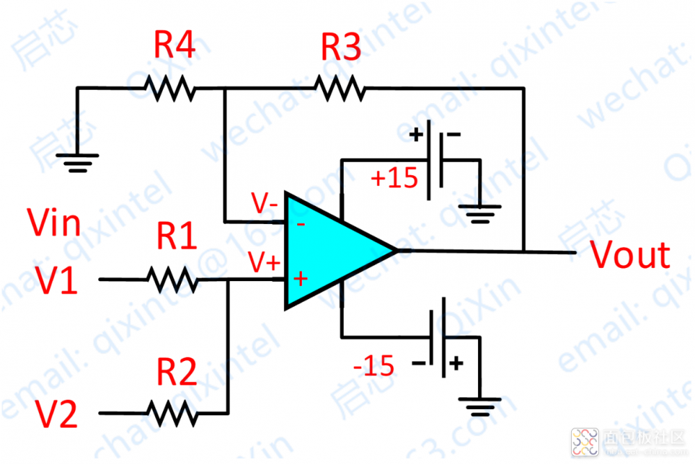
Case 4: Non-Inverting Adder
Schematic diagram of the non-inverting adder circuit (based on the OP07C low-frequency noise amplifier), with labeled input voltages V1/V2, resistors R1/R2 (input) and R3/R4 (feedback), op-amp nodes V+ (non-inverting) and V- (inverting), and output Vout
Analysis of the circuit above:
According to virtual open: no current flows through the non-inverting terminal of the op-amp, so the current through R1 is equal to the current through R2. Similarly, the current through R4 is equal to the current through R3.
Thus, we can easily derive:
——(a)
——(b)
According to virtual short: V+=V−
If the conditions R1=R2 and R3=R4 are met:
We derive from equation (a): V+=(V1+V2)/2
We derive from equation (b): V−=Vout/2
Since V+=V−, we get:
Vout=V1+V2
This is the design of a non-inverting adder.
From the above four examples, we can see that for basic op-amp circuits, no matter how their forms and connections change, as long as we master the fundamental principles of virtual short and virtual open, almost all op-amp circuits can be analyzed and solved easily!
About Maxipcb
Maxipcb empowers innovators to turn cutting-edge technologies into reality.
We offer one-stop solutions for design, simulation, testing, PCB manufacturing, component procurement and SMT assembly, enabling efficient development, rapid deployment and risk control across the full product lifecycle. Serving the world in communications, industrial automation, aerospace, automotive, semiconductor and beyond, we build a safer, more connected future together.