After the entire PCB design is completed, the circuit board needs to be mounted with components on the SMT assembly line. Each SMT manufacturing factory specifies the appropriate board size according to the processing requirements of the assembly line. If the board size is too small or too large, the fixture for fixing the board on the assembly line cannot hold it.
After the entire PCB design is completed, the circuit board needs to be mounted with components on the SMT assembly line. Each SMT manufacturing factory specifies the appropriate board size according to the processing requirements of the assembly line. If the board size is too small or too large, the fixture for fixing the board on the assembly line cannot hold it.
So what if the board size itself is smaller than the factory-specified size? It is necessary to panelize the board, combining multiple boards into one large panel. Panelization can significantly improve efficiency for both high-speed placement machines and wave soldering. The main purposes of panelization are to reduce material waste and improve production efficiency.
Starting from SPB 17.4, Cadence has included the Fab Panelization Tool as a basic function of PCB Editor, allowing designers to quickly implement mixed panelization design directly in the Allegro PCB Editor environment after completing single-board design, so as to optimize the manufacturing process.
In the previous two issues, we introduced single-board panelization and mixed panelization design.
This article describes how to output processing data and silkscreen after panelization.During panelization design, the system automatically generates a new Netlist and Refdes to ensure no conflicts in panel data. The system defines a new attribute Panel ID for each module as the identifier of the module entity. During the instantiation process of modules, the new attribute Panel ID is used as the prefix of Logic (nets and components) to define new names.
After panelization design, when defining Artwork, you can no longer use the information in Refdes-Silkscreen used in single-board design. Instead, you need to use the newly created information layer PACKAGE GEOMETRY - Pnl_Refdes.
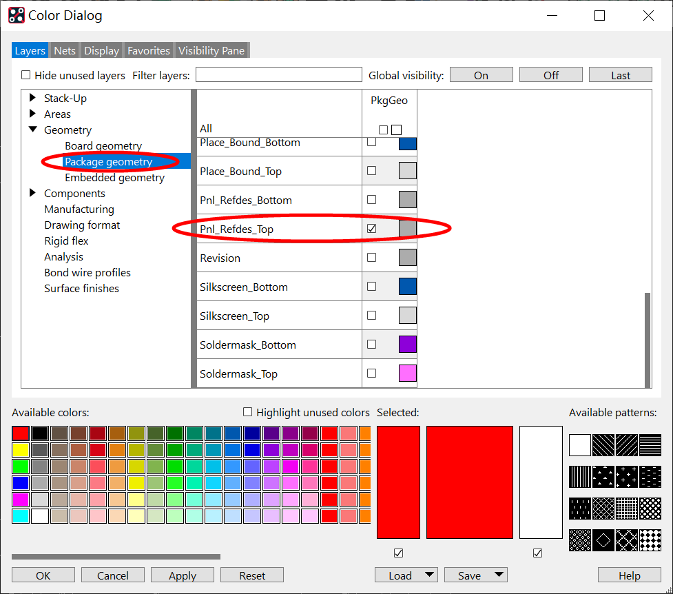
When outputting silkscreen after panelization, please note that you should select Panel Refdes, Top or Bottom. For the top layer, select
Pnl_Refdes_Top:
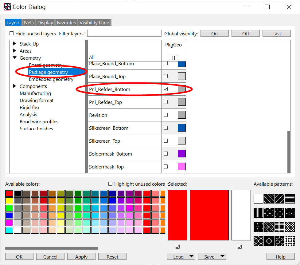
If you set the bottom layer, select
Pnl_Refdes_Bottom:
Now we start setting up silkscreen layer data output:
01 Set Top Silkscreen
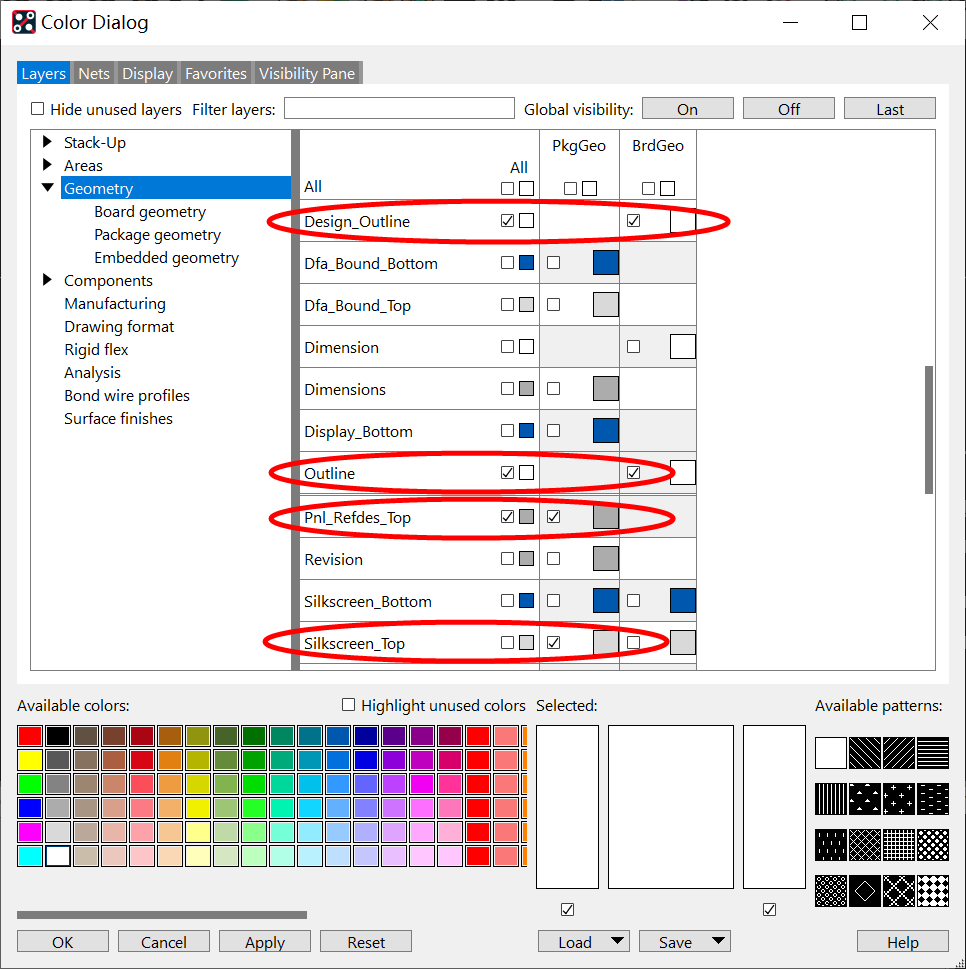
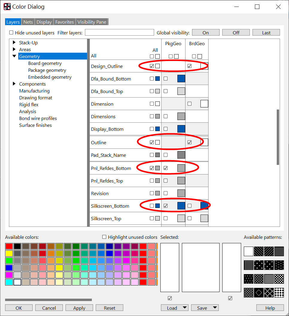
First, open the Color settings interface, turn off all information layers first, then select the layers to be output. For the top silkscreen, we generally need to include the following layers:
- Package Geometry – Silkscreen_Top
- Package Geometry – Pnl_Refdes_Top
- Board Geometry – Design_outline
- Board Geometry – Outline
After selection, only the contents of the selected layers are displayed on the canvas.
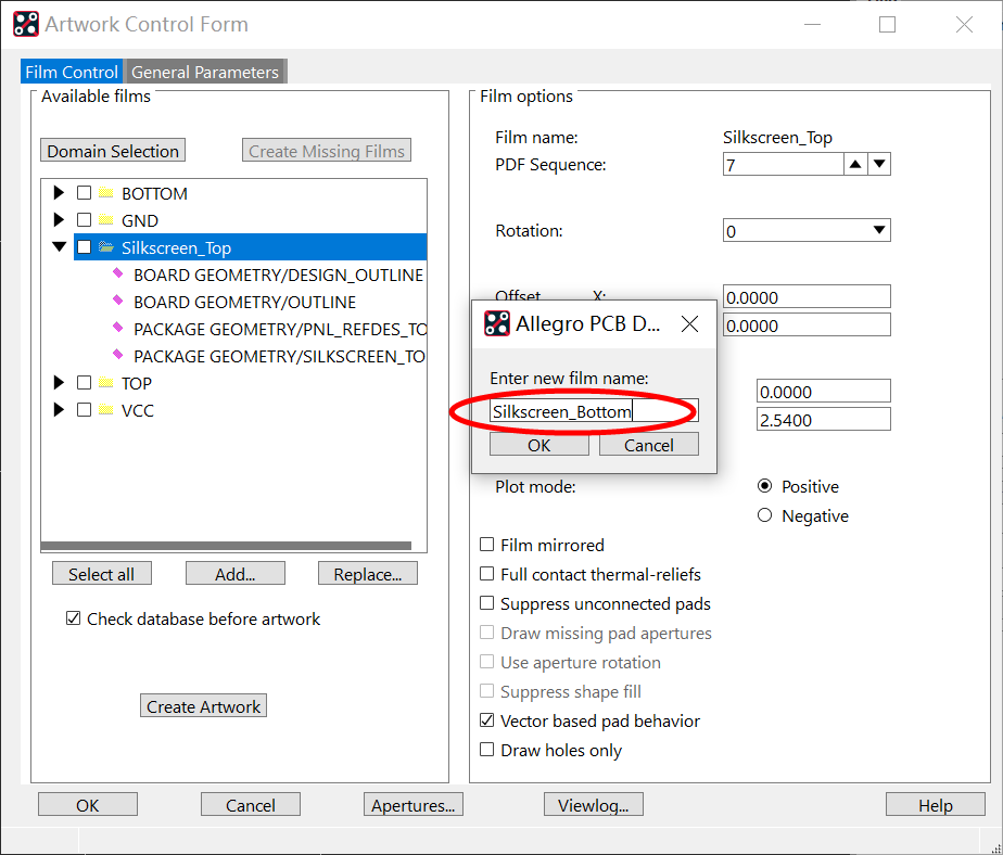
02 Set Artwork
Open
Artwork under the
Manufacturer menu. Right-click in the photoplot data area and click
Add. Enter
Silkscreen_Top in the name field, then click
OK.
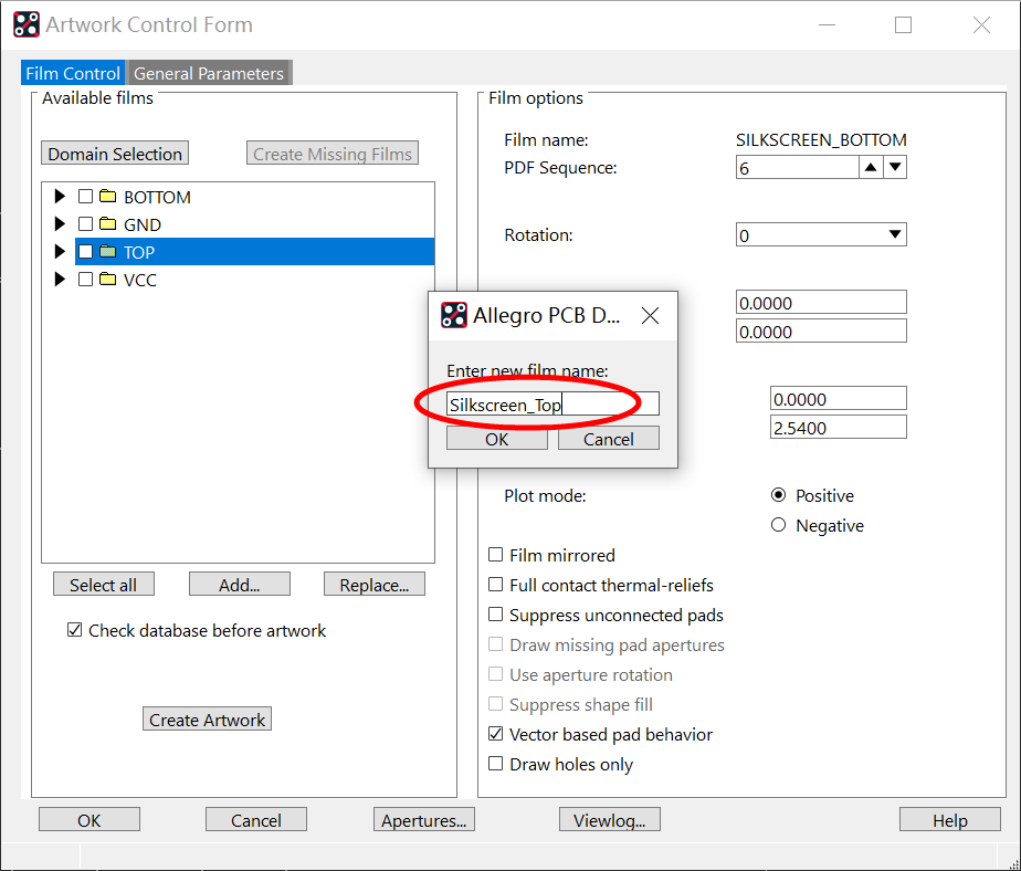
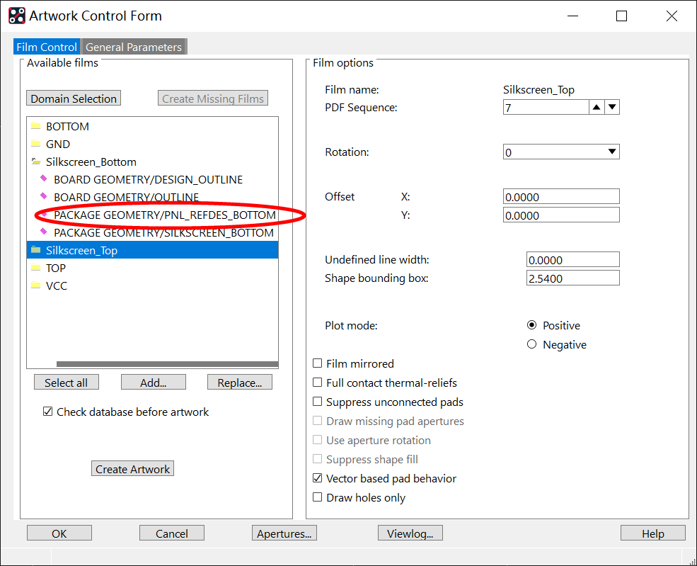
After adding successfully, expand
Silkscreen_Top, then confirm whether the silkscreen layer information is consistent with your selection:

03 Set Bottom Silkscreen
After completing the top silkscreen setup, open the Color settings interface again, replace the top silkscreen layers with bottom silkscreen layers, and perform bottom silkscreen data setup. After selection, only the newly selected layers are displayed on the canvas.
04 Set Artwork
Switch back to the Artwork setup interface. Right-click in the photoplot data area and click
Add. Enter
Silkscreen_Bottom in the name field, then click
OK.
After adding successfully, expand
Silkscreen_Bottom, then confirm whether the bottom silkscreen layer information is consistent with your selection:
Now the bottom silkscreen is added successfully. The above is the operation explanation of outputting silkscreen for panelized processing data.
About Maxipcb
Maxipcb empowers innovators to turn cutting-edge technologies into reality.
We offer one-stop solutions for design, simulation, testing, PCB manufacturing, component procurement and SMT assembly, enabling efficient development, rapid deployment and risk control across the full product lifecycle.Serving the world in communications, industrial automation, aerospace, automotive, semiconductor and beyond, we build a safer, more connected future together.


