Traditionally, digital design has been relatively straightforward. Designers could develop circuits operating at frequencies up to 30 MHz without worrying about transmission line effects, because at lower frequencies signals remain within data-specified ranges, allowing normal system operation.
1. Introduction
Traditionally, digital design has been relatively straightforward. Designers could develop circuits operating at frequencies up to 30 MHz without worrying about transmission line effects, because at lower frequencies signals remain within data-specified ranges, allowing normal system operation. However, as system performance improves, designers face greater challenges—higher frequencies impose analog effects on the system, requiring designers to consider not only digital characteristics but also analog behavior within the system.
Some of the biggest design challenges relate to I/O signals, where transmission line effects can significantly impact transmitted data. At low speeds, frequency response has little effect on signals unless the transmission medium is extremely long. As speed increases, high-frequency effects dominate; even the shortest traces suffer from ringing, crosstalk, reflection, and ground bounce, severely degrading signal response and destroying signal integrity. In practice, these issues can be overcome with good design techniques and simple layout guidelines. Altera provides information to help address these problems.
Transmission Line Effects
A transmission line is a connection that carries signals between a transmitter and a receiver. Traditionally, transmission lines were regarded as telecommunication cables for long‑distance use. With high‑speed digital signaling, even the shortest passive PCB traces are subject to transmission line effects.
At low frequencies, wires or PCB traces can be treated as ideal conductors with no resistance, capacitance, or inductance. At high frequencies, AC circuit characteristics dominate, making impedance, inductance, and capacitance inherent in conductors. As shown in Figure 1 below, an equivalent circuit model can be derived to determine the characteristic impedance of a wire or trace. This impedance is critical, as any mismatch in the transmission path degrades signal quality.
Impedance Mismatch
Impedance mismatch occurs when the source output impedance (ZS), line impedance (ZO), and receiver/load impedance (ZL) are not equal. Transmitted signals are not fully absorbed at the receiver, and excess energy reflects back to the transmitter. This process repeats until all energy is absorbed. At high data rates, this causes dangerous signal degradation: overshoot, undershoot, ringing, and staircasing, all of which introduce errors.
Impedance mismatch is resolved by matching transceiver buffers to the transmission medium. For PCBs, this is achieved through careful dielectric selection and proper termination schemes.
Impedance mismatch causing signal reflection
Various termination methods can solve this problem depending on the application. These include simple parallel termination for Stratix GX devices (shown in Figure 2), as well as more complex RC termination, where the RC network acts as a low‑pass filter to suppress low‑frequency effects while passing high‑frequency signals.
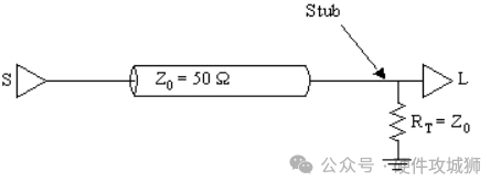
Figure 2 – Parallel termination example for Stratix GX
While external components often improve performance, they consume board space and may require stubs that introduce new problems.
Intel FPGA high‑speed I/O solutions offer on‑chip programmable termination to reduce reliance on external parts. Stratix and Stratix GX devices include on‑chip termination technology, providing driver and receiver impedance matching for serial and differential I/O. High‑speed transceiver blocks on Stratix GX devices add an internal programmable termination scheme supporting most high‑speed I/O standards. Beyond termination, sound PCB design techniques overcome these issues.
2. Signal Attenuation
High‑frequency signals experience loss along transmission lines, impairing the receiver’s ability to interpret data. Table 1 lists causes of loss in transmission media.
Table 1. Causes of Transmission Line Loss
| Cause |
Description |
| Dielectric Absorption |
High‑frequency signals excite molecules in insulators, causing them to absorb signal energy and reduce amplitude. This depends on PCB material and can be improved by material selection. |
| Skin Effect |
Time‑varying AC/high‑frequency current flows near the conductor surface. Self‑inductance creates higher reactance at high frequencies, confining electrons to the surface. Reduced effective conduction area increases resistance and attenuates signals. Wider traces reduce skin effect but are not always feasible. |
Figure 3 – Skin effect in high‑frequency conductors
Crosstalk
A signal driven along a trace generates a surrounding magnetic field. When two traces are adjacent, their fields interact, causing energy coupling between signals—known as crosstalk. Table 3 describes the primary coupling mechanisms.
Table 3. Coupling Types Causing Crosstalk
| Coupling |
Description |
| Mutual Inductance |
Induced current from the aggressor net appears on the victim net via magnetic fields. It creates a positive pulse at the near end (near the transmitter) and a negative pulse at the far end (near the receiver). |
| Mutual Capacitance |
Electric‑field coupling injects current proportional to voltage slew rate into the victim net, creating positive pulses at both ends of the transmission line. |
Careful PCB design greatly reduces crosstalk. Methods for microstrip and stripline layouts:
- Increase spacing between signal traces as much as routing constraints allow
- Route traces close to the ground plane for tight coupling and isolation
- Use differential routing, especially for critical nets
- Place signals on separate layers and route orthogonally if coupling is significant
- Minimize parallel run lengths between signals
3. Simultaneous Switching Outputs (SSO)
As digital circuit speed rises, output switching times shorten. Faster switching discharges load capacitance more rapidly, creating larger transient currents in outputs. When multiple outputs switch from high to low simultaneously, charge stored in I/O load capacitors flows into the device. This sudden current exits the chip through internal inductance to the board ground, generating a voltage difference between the die ground and the PCB ground. This temporarily raises the I/O low‑level voltage above the true ground plane—a phenomenon called ground bounce. Ground bounce can cause an output low to be interpreted as a logic high by other devices.
Ground bounce can be reduced by following board‑level design rules in AN 315: High‑Speed FPGA PCB Design Guidelines. Altera high‑speed solutions offer pin slew‑rate control to lower driver speed and mitigate bounce. These devices also include multiple power and ground pins, allowing high‑speed I/Os to be placed near ground pins to reduce SSO effects.
Addressing high‑speed design challenges requires extra effort to ensure signal integrity. This is achievable by following basic analog design rules and careful PCB layout. Altera high‑speed programmable logic devices include many features—programmable slew‑rate control, on‑chip termination—to simplify high‑speed design.
About Maxipcb
Maxipcb empowers innovators to turn cutting-edge technologies into reality.
We offer one-stop solutions for design, simulation, testing, PCB manufacturing, component procurement and SMT assembly, enabling efficient development, rapid deployment and risk control across the full product lifecycle.Serving the world in communications, industrial automation, aerospace, automotive, semiconductor and beyond, we build a safer, more connected future together.


