Precision PCB Fabrication, High-Frequency PCB, High-Speed PCB, Standard PCB, Multilayer PCB and PCB Assembly. The most reliable PCB&PCBA custom service factory
Precision PCB Fabrication, High-Frequency PCB, High-Speed PCB, Standard PCB, Multilayer PCB and PCB Assembly. The most reliable PCB&PCBA custom service factory
Home > News > PCB LAYOUT > Impedance Regulation Strategies for PCB Traces
Without impedance control, significant signal reflection and distortion will occur, leading to design failure. Common signals such as PCI bus, PCI-E bus, USB, Ethernet, DDR memory, and LVDS signals all require impedance control. Ultimately, impedance control is achieved through PCB design, which imposes higher requirements on PCB manufacturing processes.
Mar 31st,202637 Views
Without impedance control, significant signal reflection and distortion will occur, leading to design failure. Common signals such as PCI bus, PCI-E bus, USB, Ethernet, DDR memory, and LVDS signals all require impedance control. Ultimately, impedance control is achieved through PCB design, which imposes higher requirements on PCB manufacturing processes. By communicating with PCB manufacturers and using EDA software, trace impedance can be controlled in accordance with signal integrity requirements.
The impedance value of different routing methods can be calculated accurately.
1. Microstrip Line
A microstrip line consists of a strip conductor and a ground plane, with a dielectric layer in between. If the dielectric constant of the medium, the width of the line, and the distance from the line to the ground plane are controllable, its characteristic impedance is also controllable with an accuracy of ±5%.
Microstrip line structure diagram (strip conductor, dielectric layer, ground plane labeled with parameters W, H, εr)
2. Stripline
A stripline is a copper strip placed in the middle of a dielectric layer between two conductive planes. If the thickness and width of the line, the dielectric constant of the medium, and the distance between the two ground planes are controllable, the characteristic impedance of the line is also controllable with an accuracy of ±10%.
Characteristic impedance formula for stripline:
Z0=εr60ln[π(0.8w+t)5.98b]
This formula is sufficiently accurate when w/(b−t)<0.35 and t/b<0.25.
Transmission delay of stripline:
tpd=1.017εr ns/ft
For FR-4 boards (εr=4.5), the signal transmission speed is approximately 12 cm/ns. Similarly, the transmission delay is independent of line width or spacing.
To achieve effective impedance control, it is first necessary to understand the structure of multilayer PCBs:
A typical multilayer PCB is formed by laminating core boards and prepregs. Core boards are rigid, specific-thickness boards with copper cladding on both sides, serving as the base material of the printed board. Prepregs form the so-called bonding layer to adhere core boards; although they have an initial thickness, their thickness changes during the lamination process.
The outermost two dielectric layers of a multilayer PCB are usually prepregs, with separate copper foil layers as outer copper cladding. The original thickness specifications of outer and inner copper foils are generally 0.5 oz, 1 oz, and 2 oz (1 oz ≈ 35 μm or 1.4 mil). After a series of surface treatments, the final thickness of the outer copper foil generally increases by nearly 1 oz. The inner copper foil is the copper cladding on both sides of the core board, and its final thickness differs slightly from the original thickness but generally decreases by a few micrometers due to etching.
The outermost layer of a multilayer PCB is the solder mask (commonly known as "green oil," which can also be yellow or other colors). The thickness of the solder mask is generally not easy to determine accurately—it is slightly thicker in areas without copper foil than in areas with copper foil. However, due to the absence of copper foil thickness, the copper foil still appears more prominent, which can be felt when touching the surface of the printed board.
When manufacturing a printed board of a specific thickness, it is necessary to reasonably select parameters of various materials, and the final thickness of the prepreg will be slightly smaller than the initial thickness. Below is a typical 6-layer PCB stackup structure:
4. PCB Parameters
PCB parameters vary slightly among different manufacturers. Through communication with the technical support of the circuit board manufacturer, the following parameter data of the manufacturer is obtained:
(1) Outer Copper Foil
Available original thicknesses: 12 μm, 18 μm, 35 μm.
Final thickness after processing: approximately 44 μm, 50 μm, 67 μm.
(2) Core Board
Commonly used material: S1141A (standard FR-4) with copper cladding on both sides. Available specifications can be confirmed with the manufacturer.
(3) Prepreg
Specifications (original thickness):
7628: 0.185 mm
2116: 0.105 mm
1080: 0.075 mm
3313: 0.095 mm
The actual thickness after lamination is usually 10–15 μm smaller than the original value. A maximum of 3 prepregs can be used for the same bonding layer, and the thicknesses of the 3 prepregs cannot be the same. At least one prepreg can be used, but some manufacturers require at least two. If the thickness of the prepreg is insufficient, the copper foil on both sides of the core board can be etched away, and then the two sides can be bonded with prepregs to achieve a thicker bonding layer.
(4) Solder Mask
Thickness of solder mask on copper foil (C2): ≈8–10 μm.
Thickness of solder mask in areas without copper foil (C1): Varies with surface copper thickness. When the surface copper thickness is 45 μm, C1≈13–15 μm; when the surface copper thickness is 70 μm, C1≈17–18 μm.
(5) Conductor Cross-Section
The cross-section of a conductor is actually trapezoidal (not rectangular as commonly assumed). Taking the TOP layer as an example, when the copper foil thickness is 1 oz, the upper base of the trapezoid is 1 mil shorter than the lower base. For example, a 5-mil line width has an upper base of approximately 4 mil and a lower base of 5 mil. The difference between the upper and lower bases is related to the copper thickness. The following table shows the relationship between the upper and lower bases of the trapezoid under different conditions:
Layer
Base Copper Thickness (μm)
Upper Line Width (mil)
Lower Line Width (mil)
Inner Layer
18
W0−0.5
W0
35
W0−1
W0
70
W0−1.5
W0−1
Outer Layer
18
W0−1
W0
35
W0−0.8
W0−0.5
70
W0−1.2
W0−0.8
Note: W0 denotes the designed line width.
(6) Dielectric Constant
The dielectric constant of prepreg is related to its thickness. The following table shows the thickness and dielectric constant parameters of different types of prepregs:
Model
Thickness (mil)
Dielectric Constant (εr)
1080
2.8
4.3
3313
3.8
4.3
2116
4.5
4.5
7628
6.8
4.0
The dielectric constant of the material is related to its resin composition. The dielectric constant of FR-4 ranges from 4.2 to 4.7 and decreases with increasing frequency.
(7) Dielectric Loss Factor
The energy consumed by a dielectric material due to heating under an alternating electric field is called dielectric loss, usually expressed by the dielectric loss factor tanδ. The typical value of S1141A is 0.015.
(8) Minimum Processable Line Width and Spacing
4 mil/4 mil (line width/line spacing).
5. Introduction to Impedance Calculation Tools
After understanding the multilayer PCB structure and mastering the required parameters, impedance can be calculated using EDA software. Allegro can be used for this purpose, but another tool—Polar SI9000—is recommended here. It is an excellent tool for calculating characteristic impedance and is widely used by many printed board manufacturers.
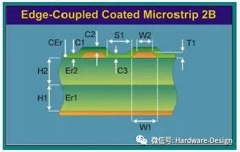
For both differential and single-ended lines, the calculation results of Polar SI9000 and Allegro show only slight differences when calculating the characteristic impedance of inner-layer signals, which is related to the handling of details such as the shape of the conductor cross-section. However, when calculating the characteristic impedance of outer-layer signals, it is recommended to select the Coated model instead of the Surface model, as the former considers the presence of the solder mask, resulting in more accurate results.
Screenshot of Polar SI9000 calculating outer-layer differential line impedance with solder mask considered (Edge-Coupled Coated Microstrip model)
Since the thickness of the solder mask is not easy to control, an approximate method can be used according to the manufacturer's suggestions: subtract a specific value from the result calculated by the Surface model—recommend subtracting 8 ohms for differential impedance and 2 ohms for single-ended impedance.
6. PCB Requirements for Differential Pair Routing
(1) Determine Routing Mode, Parameters, and Impedance Calculation
Differential pair routing is divided into two modes: outer-layer microstrip differential mode and inner-layer stripline differential mode. By setting parameters reasonably, impedance can be calculated using relevant impedance calculation software (such as POLAR-SI9000) or impedance calculation formulas.
(2) Route Parallel and Equally Spaced Lines
Determine the routing line width and spacing. During routing, strictly follow the calculated line width and spacing, and keep the spacing between the two lines constant (i.e., maintain parallelism). There are two parallel methods:
Side-by-side: Two lines are routed on the same layer.
Over-under: Two lines are routed on upper and lower adjacent layers.
It is generally advisable to avoid the latter (interlayer differential signals), because during the actual PCB manufacturing process, the lamination alignment accuracy between layers is much lower than the same-layer etching accuracy, and dielectric loss during lamination cannot guarantee that the spacing of differential lines is equal to the interlayer dielectric thickness, which will cause changes in the differential impedance of interlayer differential pairs. Therefore, it is recommended to use same-layer differential routing as much as possible.
About Maxipcb
Maxipcb empowers innovators to turn cutting-edge technologies into reality.
We offer one-stop solutions for design, simulation, testing, PCB manufacturing, component procurement and SMT assembly, enabling efficient development, rapid deployment and risk control across the full product lifecycle. Serving the world in communications, industrial automation, aerospace, automotive, semiconductor and beyond, we build a safer, more connected future together.